Intel's 32nm Update: The Follow-on to Core i7 and More
by Anand Lal Shimpi on February 11, 2009 12:00 AM EST- Posted in
- CPUs
Fat Pockets, Dense Cache, Bad Pun
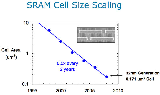
Whenever Intel introduces a new manufacturing process the first thing we see it used on is a big chip of cache. The good ol’ SRAM test vehicle is a great way to iron out early bugs in the manufacturing process and at the end of 2007 Intel demonstrated its first 32nm SRAM test chip.
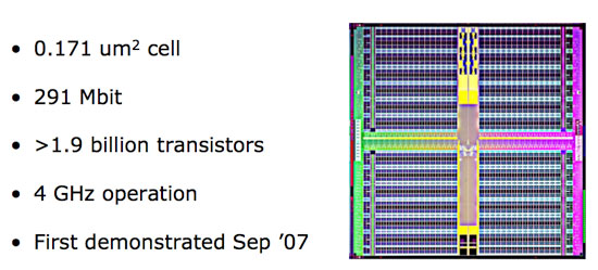
Intel's 32nm SRAM test vehicle
The 291Mbit chip was made up of over 1.9 billion transistors, switching at 4GHz, using Intel’s 32nm process. The important number to look at is the cell size, which is the physical area a single bit of cache will occupy. At 45nm that cell size was 0.346 um^2 (for desktop processors, Atom uses a slightly larger cell), compared to 0.370 um^2 for AMD’s 45nm SRAM cell size. At 32nm you can cut the area nearly in half down to 0.171 um^2 for a 6T SRAM cell. This means that in the same die area Intel can fit twice the cache, or the same amount of cache in half the area. Given that Core i7 is a fairly large chip at 263 mm^2 I’d expect Intel to take the die size savings and run with them. Perhaps with a modest increase to L3 cache size.
A big reason we’re even getting this disclosure today is because of how healthy the 32nm process is. Below we have a graph of defect density (number of defects in silicon per area) vs time; manufacturing can’t start until you’re at the lowest part of that graph - the tail that starts to flatten out:
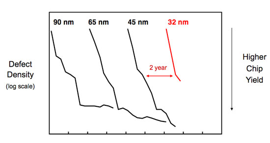
Intel’s 45nm process ramped and matured very well as you can see from the chart. The 45nm process reached lower defect densities than both 65nm and 90nm and did it faster than either process. Intel’s 32nm process is on track to outperform even that.
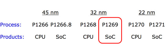
Two Different 32nm Processes?
With Intel now getting into the SoC business (System on a Chip), each process node will now have two derivatives - one for CPUs and one for SoCs. This started at 45nm with process P1266.8, used for Intel’s consumer electronics and Moorestown CPUs and will continue at 32nm with the P1269 process.
There are two major differences between the CPU and SoC versions of a given manufacturing process. One, the SoC version will be optimized for low leakage while the CPU version will be optimized for high drive current. Remember that graph comparing leakage vs. drive current of 45nm vs. 32nm? The P1268 process will exploit the arrows to the right, while P1269 will attempt to push leakage current down.
The second difference is that certain SoC circuits require higher than normal voltages and thus you need a process that can tolerate those voltages. Remember that with a SoC it’s not always just Intel IP being used, there are many third parties that will contribute to the chips that eventually make their way into smartphones and other ultra portable devices.
The buck doesn’t stop here, in two more years we’ll see the introduction of P1270, Intel’s 22nm process. But before we get there, there’s a little stop called Sandy Bridge. Let’s talk about microprocessors for a bit now shall we?


64 Comments
View All Comments
tacoburrito - Wednesday, February 11, 2009 - link
I fail to see the purpose of introducing the 6 core/Gulfstream. Most software could barely take advantage of 4 core, let alone 6. It seems like Intel just want to brag they can cram many cores into a single package without evidence that 6 cores will improve performance. It's almost like the mhz wars from the 1990s. Instead of spending time on a 6 core chip, why couldn't they just bring out Sandy Bridge earlier?aeternitas - Friday, February 13, 2009 - link
It cant be that the applications that DO have multicore support arnt professional apps that small and large businesses use to make money now could it?Simple because Intel doesn't cater to your browsing and downloading torrents needs doesn't mean its not a good idea to get the ball rolling.
Oh and hmm, lets see why don't they just go strait to Sandy Bridge that's a good one hmmm maybe its because they DONT HAVE TO. AMD is 18 months behind.
7Enigma - Thursday, February 12, 2009 - link
Check back a couple pages, I think we posted exactly the same thing, as I completely agree with you. :)The only thing I can think of is since the server market pays the bills in a sense they are tailoring the chip for that purpose and just making a consumer level chip that will still be tops but probably not as nice in most instances as a faster quad.
pattycake0147 - Wednesday, February 11, 2009 - link
On the first page the article talks about two Arizona fabs, but the picture indicates that there is one Arizona fab and one New Mexico fab. So which is correct?scruffypup - Wednesday, February 11, 2009 - link
If I remember right (living here in the Phoenix area), there are 3 buildings in Chandler at the site,... 2 of them will be coverted over to the 32nm process, the 3rd building is no longer going to be used apparently,.... or will use the 3rd for something else,...http://www.intel.com/community/arizona/index.htm">http://www.intel.com/community/arizona/index.htm
http://www.azcentral.com/arizonarepublic/business/...">http://www.azcentral.com/arizonarepubli.../2009/02...
"Specifically, Intel is upgrading two of its three manufacturing plants, called "fabs," at its Ocotillo campus in Chandler to make 32-nanometer-size chips."
INDVote - Thursday, February 12, 2009 - link
No, only one fab in AZ is being converted, Intel's newest Fab 32. They are not closing any one or both other buildings. They appear to be "merging" two of them.F11X is in New Mexico, and will be converted over. There are no plant closings in NM.
D1D and D1C are both at the same location in Oregon and are being converted.
pattycake0147 - Wednesday, February 11, 2009 - link
However, the three buildings combined are called Fab 32. Fab 11X as chopshiy pointed out is in New Mexico. The article isn't referring to individual buildings, but sets of buildings.Thanks chopshiy, I didn't see your post earlier.
vlado08 - Wednesday, February 11, 2009 - link
I am wondering about the integrated graphics in Clarkdale/Arrandale will it be DirectX 11 compliant? Is it going to be better than GMA X4500? What about h264 acceleration, 8 channel LPCM support and working 24p?chophshiy - Wednesday, February 11, 2009 - link
11X is in New Mexico as the caption on the pic says. Specifically Rio Rancho, NM, near Albuquerque. It's OK, you'd be surprised how many times I've spoken with someone in the US on the phone that told me I was calling the wrong number, since they don't support locations outside the US. Go American education!philosofool - Wednesday, February 11, 2009 - link
Does anyone know what the lifespan of LGA 1156 will be? Is intel expected to change sockets again when we reach Sandy Bridge? Is there any chance that I will have be able to get one mother board to last me several years?