Intel Unveils Meteor Lake Architecture: Intel 4 Heralds the Disaggregated Future of Mobile CPUs
by Gavin Bonshor on September 19, 2023 11:35 AM ESTSoC Tile, Part 2: NPU Adds a Physical AI Engine
The last major block on the SoC tile is a full-featured Neural Processing Unit (NPU), a first for Intel's client-focused processors. The NPU brings AI capabilities directly to the chip and is compatible with standardized program interfaces like OpenVINO. The architecture of the NPU itself is multi-engine in nature, which is comprised of two neural compute engines that can either collaborate on a single task or operate independently. This flexibility is crucial for diverse workloads and potentially benefits future workloads that haven't yet been optimized for AI situations or are in the process of being developed. Two primary components of these neural compute engines stand out: the Inference Pipeline and the SHAVE DSP.
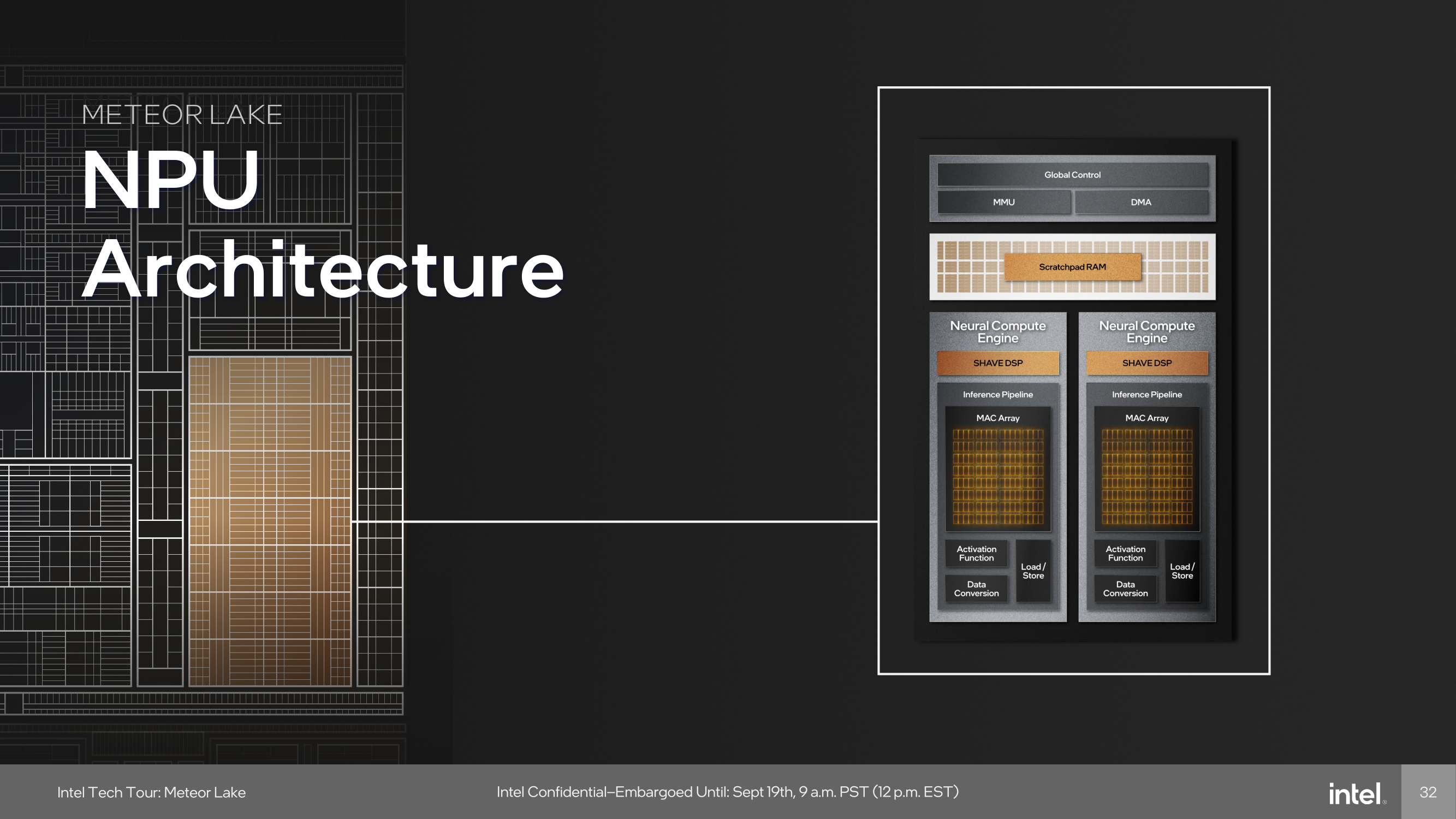
The Inference Pipeline is primarily responsible for executing workloads in neural network execution. It minimizes data movement and focuses on fixed-function operations for tasks that require high computational power. The pipeline comprises a sizable array of Multiply Accumulate (MAC) units, an activation function block, and a data conversion block. In essence, the inference pipeline is a dedicated block optimized for ultra-dense matrix math.
The SHAVE DSP, or Streaming Hybrid Architecture Vector Engine, is designed specifically for AI applications and workloads. It has the capability to be pipelined along with the Inference Pipeline and the Direct Memory Access (DMA) engine, thereby enabling parallel computing on the NPU to improve overall performance. The DMA Engine is designed to efficiently manage data movement, contributing to the system's overall performance.
At the heart of device management, the NPU is designed to be fully compatible with Microsoft's new compute driver model, known as MCDM. This isn't merely a feature, but it's an optimized implementation with a strong emphasis on security. The Memory Management Unit (MMU) complements this by offering multi-context isolation and facilitates rapid and power-efficient transitions between different power states and workloads.
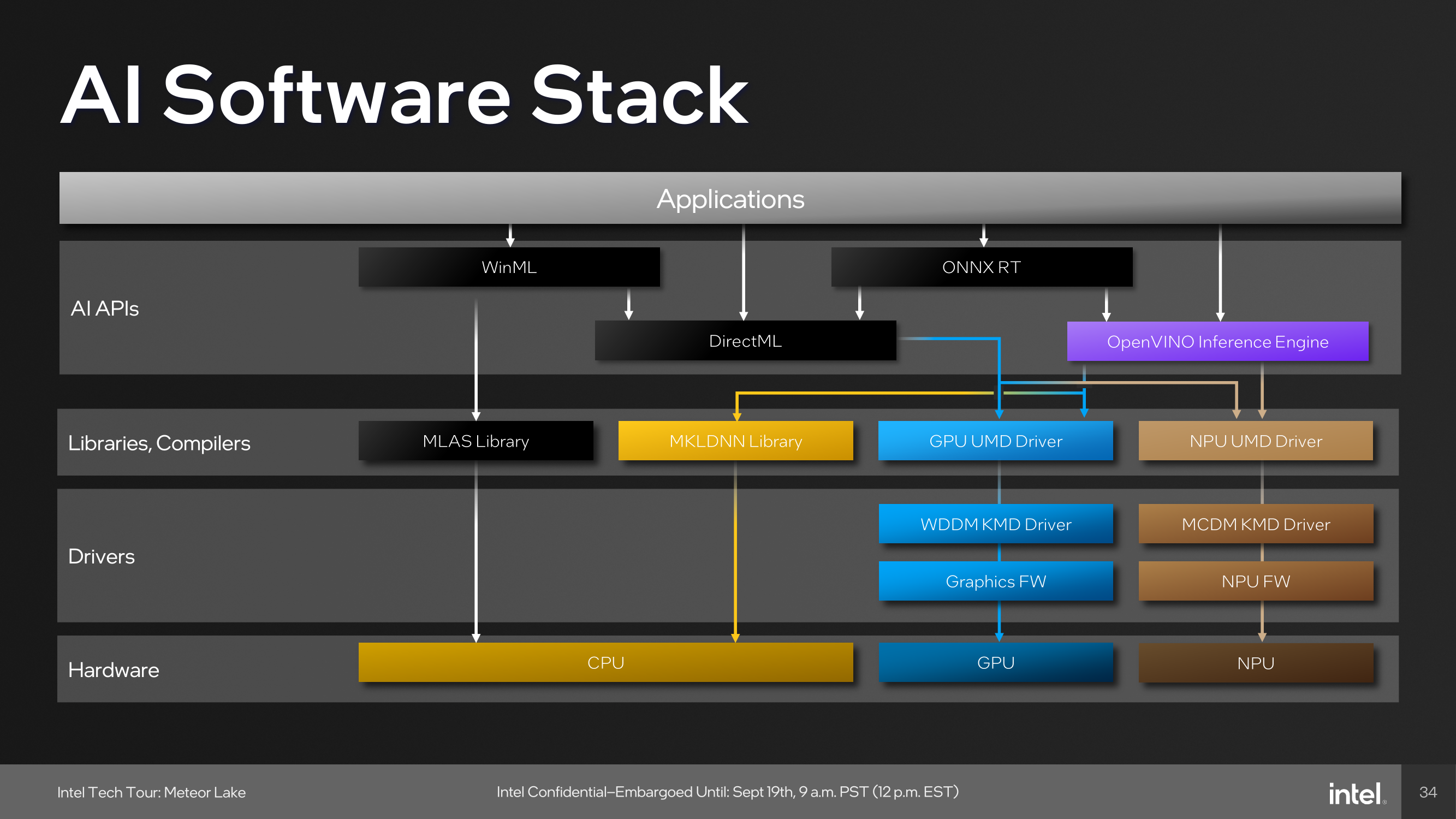
As part of building an ecosystem that can capitalize on Intel's NPU, they have been embracing developers with a number of tools. One of these is the open-source OpenVINO toolkit, which supports various models such as TensorFlow, PyTorch, and Caffe. Supported APIs include Windows Machine Learning (WinML), which also includes the DirectML component of the library, the ONNX Runtime accelerator, and OpenVINO.
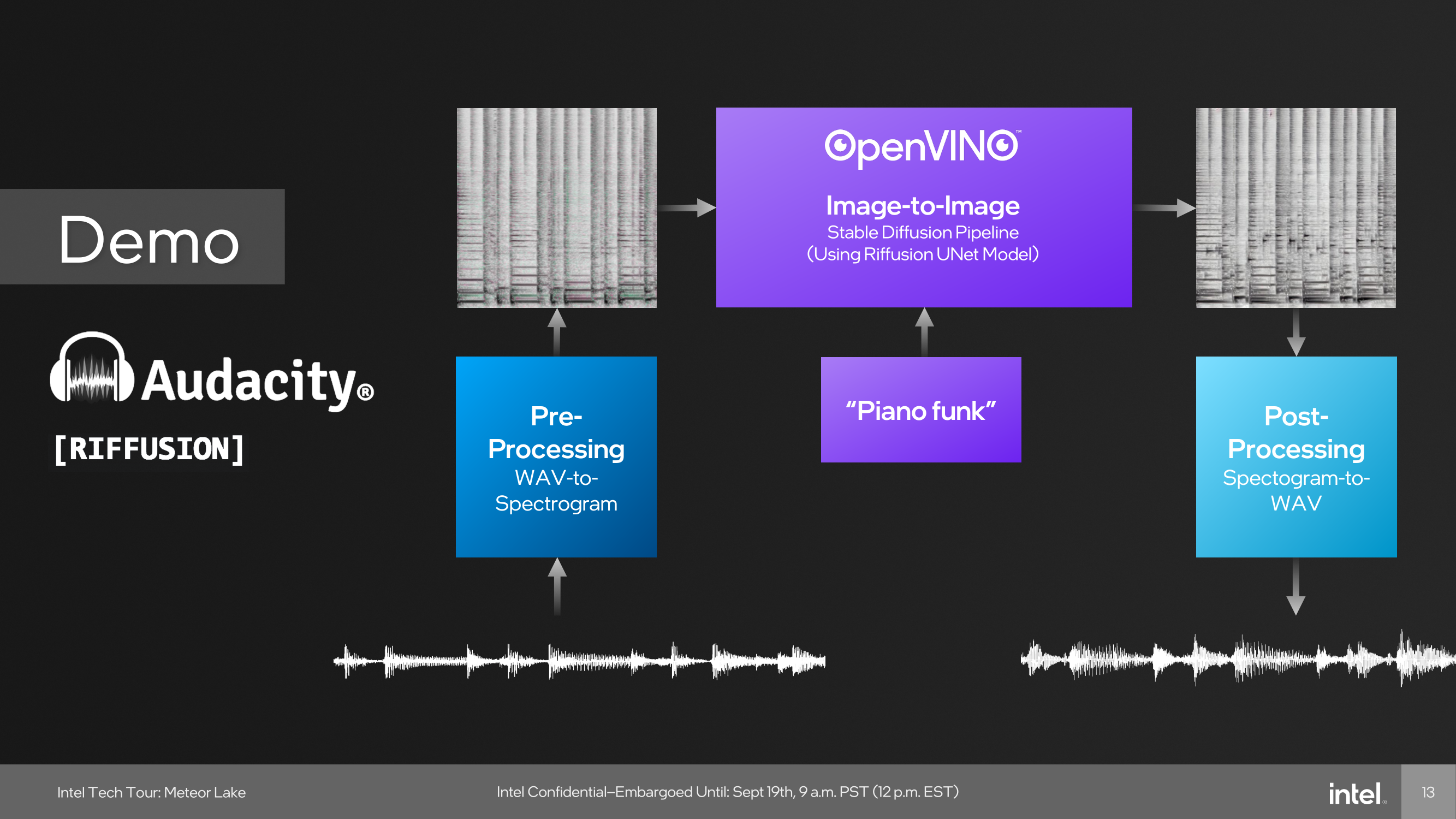
One example of the capabilities of the NPU was provided through a demo using Audacity during Intel's Tech Tour in Penang, Malaysia. During this live demo, Intel Fellow Tom Peterson, used Audacity to showcase a new plugin called Riffusion. This fed a funky audio track with vocals through Audacity and separated the audio tracks into two, vocals and music. Using the Riffusion plugin to separate the tracks, Tom Peterson was then able to change the style of the music audio track to a dance track.
The Riffusion plugin for Audacity uses Stable Diffusion, which is an open-source AI model that traditionally generates images from text. Riffusion goes one step further by generating images of spectrograms, which can then be converted into audio. We touch on Riffusion and Stable Diffusion because this was Intel's primary showcase of the NPU during Intel's Tech Tour 2023 in Penang, Malaysia.

Although it did require resources from both the compute and graphics tile, everything was brought together by the NPU, which processes multiple elements to spit out an EDM-flavored track featuring the same vocals. An example of how applications pool together the various tiles include those through WinML, which has been part of Microsoft's operating systems since Windows 10, typically runs workloads with the MLAS library through the CPU, while those going through DirectML are utilized by both the CPU and GPU.
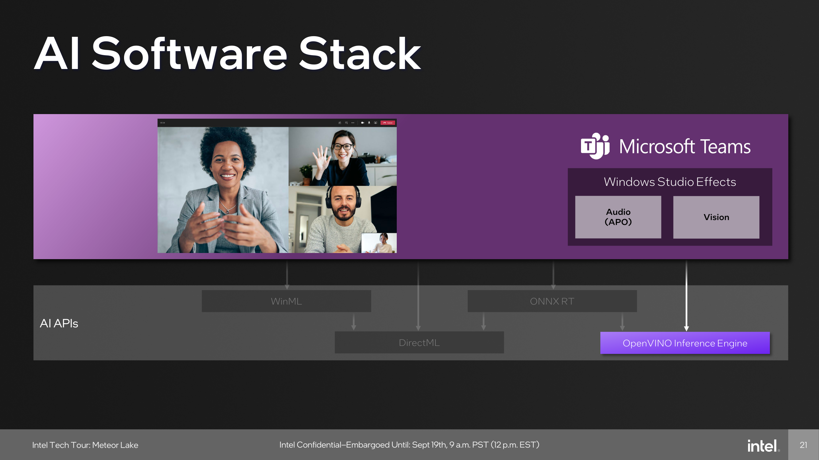
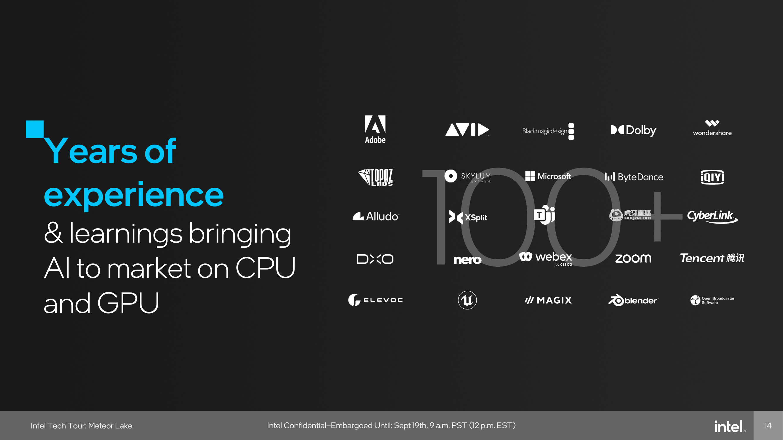
Other developers include Microsoft, which uses the capability of the NPU in tandem with the OpenVINO inferencing engine to provide cool features like speech-to-text transcripts of meetings, audio improvements such as suppressing background noise, and even enhancing backgrounds and focusing capabilities. Another big gun using AI and is supported through the NPU is Adobe, which adds a host of features for adopters of Adobe Creative applications use. These features include generative AI capabilities, including photo manipulative techniques in Photoshop such as refining hair, editing elements, and neural filters; there's a lot going on.


107 Comments
View All Comments
Composite - Thursday, September 28, 2023 - link
totally agree. At the same time, instead of doing a full Intel 4 Meteor lake chip, shrink it down to compute tile only also reduces the size of the silicon and improves yield. Later next year, Intel will also need EUV capacity for Sierra Forest and Granite Rapids. These chips will be much larger than mobile compute tile and considerably lower yield.... Intel will need every ounce of EUV capacity they have.tipoo - Tuesday, September 19, 2023 - link
Probably to have as much compute on the N4 capacity that they have, their substrate also takes much less power connecting them than current AMD and it allows for the best node for each part being used i.e if Intel's wasn't ideal for the GPU tile as the CPU tile etcComposite - Thursday, September 28, 2023 - link
I have the same question. At the same time, I was curious about Intel's EUV capacity. Since Intel is the late comer to EUV and over 50% of EUV machines are at TSMC, does Intel really have the capacity to manufacture full chip Intel 4 Meteor Lake? Not to mention up coming Sierra Forest and later on Granite Rapids will all use EUV capacity. I think the reasonable way is indeed only use EUV at the most critical part of Meteor Lake ---> Compute tile, and out source the rest.eSyr - Tuesday, September 19, 2023 - link
To avoid the issues they have with rollout 14 nm (BDW) and then 10 nm (CNL), I guess, when they held back by yield with respect to particular parts of the chip, specifically, GPU.lemurbutton - Tuesday, September 19, 2023 - link
A17 Pro just beat all Intel CPUs except the 13900KS in ST Geekbench6. A17 Pro uses less than 3w to achieve this - with typical load significantly below 3w. Meanwhile, 13900KS uses as much as 250w or more.Intel's Meteor Lake needs to improve by 10x over Raptor Lake just to match what M3 will be able to do.
Irish_adam - Tuesday, September 19, 2023 - link
The 13900ks uses 250 watts on a single core? Got a link for that?I'll think you find that single core workloads use far, far less. Also remember that benchmarks across ISA's are sketch at best and outright made up at worst. I mean just look how badly games or software can be when ported from one ISA to another, it all really comes down to how well you've made the software to run on each architecture.
Makaveli - Tuesday, September 19, 2023 - link
He is an apple fanboySource: Trust me bro!
FWhitTrampoline - Tuesday, September 19, 2023 - link
No the A17 Performance core is only clocked at 3.6/3.7GHz compared to the x86 designs that are up to clocked 2Ghz+ higher. So this is not some ESPN like Fanatic statement as since the A14/Firestorm core Apple's instruction decoder width is at least 8 decoders wide and backed up by loads of execution ports. And so Apple's P cores are of a very wide order superscalar design since the A14/Firestorm was released!And the Apple P cores are high IPC at low clocks compared to the x86 designs that have 4/6 instruction decoders so need the higher clocks to make up the IPC deficiency for single thread performance that's calculated as IPC multiplied by average sustained clocks to get that single threaded performance metric.
The lower clocks are where Apple's power savings come from and the longer battery life is obtained. That and the A17 Pro/Earlier A series SOCs have loads of specialized heterogeneous compute for offloading workloads onto instead of using the CPU cores or GPU cores so more power can be saved there for all sorts of specialized workloads. The x86 processors/SOCs are just now getting the same sorts of specialized heterogeneous compute IP blocks but that's relatively immature compare to Apple's SOCs and other ARM Based SOC ecosystems that have been using that specialized heterogeneous compute IP for years now.
GeoffreyA - Thursday, September 21, 2023 - link
Well, it would be interesting to see Intel or AMD make a fixed-width ISA design and how that then stacks up against the stuff of Apple. Really, x86 is at a disadvantage because of the variable-width instructions but still has done a fantastic job. Or, I'd like to see Apple design an x86 CPU and see how that holds up against Zen and the rest.FWhitTrampoline - Thursday, September 21, 2023 - link
No logical reason for Apple to go CISC as the x86 Instruction Decoder requires many times the transistors to implement than the transistors required to implement a RISC ISA Instruction Decoder! So it was easy to get 8 Instruction Decoders to fit on the front of the A14/Firestorm processor core(RISC ISA Based). It's easier to go wider if one has a relatively fewer Instructions of a fixed length to implement in a Instruction Decoder design. So that makes it easy to produce a custom very wide order superscalar processor core design that targets high IPC at a lower clock rate and the SOC's CPU cores clocked well inside their Performance/Watt sweet spot. And to still have that A14 match/get close to the x86 cores in single threaded performance and against x86 core designs that are clocked 2GHz+ higher.The x86 ISA is too Legacy Instructions bloated and it's not going to be easy to refactor that and not require years in the process to do that. The ARM ISA ecosystem is from the ground up RISC there and even though the x86 designers have a RISC like back end to break those CISC down into more RISC like instructions, that hardware engine take more transistors to implement and thus will use more power resources getting that done. The vast majority of ARM ISA instructions translate 1 to 1 into single and some a few Micro-OPs so how hard is that to decode compared to x86 ISA instruction that mostly have multiple micro-ops generated to get all that complex work done. And there's a valid power usage reason that x86 never made any inroads into the wider tablet/smartphone market.
The thing about the ARM/RISC core designs is that they can scale from phones to server/HPC whereas the CISC designs can not scale down as low power as RISC designs! but Intel has done a good job at getting close there but a little too late to matter to the OEMs that really did not want to remain beholden to Intel and x86. And the same can be said now for RISC-V compared to an ARM Holdings that's maybe leaning more towards an x86 like business model where RISC-V represents total end user ISA freedom there, within reason, as the RISC-V ISA is totally open not royalist/encumberments required/enforced.