Intel Unveils Meteor Lake Architecture: Intel 4 Heralds the Disaggregated Future of Mobile CPUs
by Gavin Bonshor on September 19, 2023 11:35 AM ESTSoC Tile, Part 3: Disaggregating Xe Media and Display Engine From Graphics
As we noted earlier, Intel has completely redesigned its graphics, media, and display engine for Meteor Lake and, as such, separates all three entities from each other. While we'll cover the new graphics tile next, we'll start with everything that's not part of the graphics tile. Opting for a disaggregated architecture allows Intel to not only shuffle things around from an IP perspective but also allows Intel to integrate new IPs such as cores, graphics, and I/O as and when advancements have been made at a silicon level, but the design allows unties Intel from being limited to a specific manufacturing process.

Starting things off, we have the Xe Media Engine, which is embedded within the SoC tile. Within the Xe Media Engine are two Multi-Format Codecs (MFX), designed and responsible for all the encoding and decoding tasks. Intel's Meteor Lake with Xe supports the latest codecs ranging from AV1 (decode and encode), HEVC, AVC, and VP9, with up to 8K60 HDR decode supported. For encoding, there's support for up to 8K resolutions with 10-bit color and HDR. Aiming to improve power efficiency on-chip with encode/decode workloads, having a dedicated Media Engine separate from the graphics allows Intel to find granular power savings as things are directed to the Xe Media Engine, which means the graphics tile doesn't need to be powered up to accomplish encode or decode tasks.

The Xe Media Engine provides various functionalities across a large spectrum of different video codecs. This ranges from JPEG/MPEG and AVC to the more advanced VP9, HEVC, and AV1 codecs. Designed to give Meteor Lake a solid level of computational efficiency for video processing, the Xe Media Engine balances the gaps between high-performance output and power efficiency, rendering it particularly well-suited for various applications, from real-time video streaming to high-fidelity playback. There's also support for diverse color formats and bit depths, including but not limited to 4:2:0 at 10-bit and 12-bit, which means it's versatile for video editing and video encoding and should satisfy content creator's needs.
Xe Display Engine: Also Within the SoC
Much like the Xe Media Engine, the Xe Display Engine is also found within the SoC tile on Meteor Lake. Decoupling this directly from the graphics tile and embedded into the SoC allows it to communicate directly with the Xe Media Engine, saving power and improving overall battery life. The engine supports up to four display pipes, two of which have been designed and optimized for low power consumption, further boosting overall efficiency for Meteor Lake.
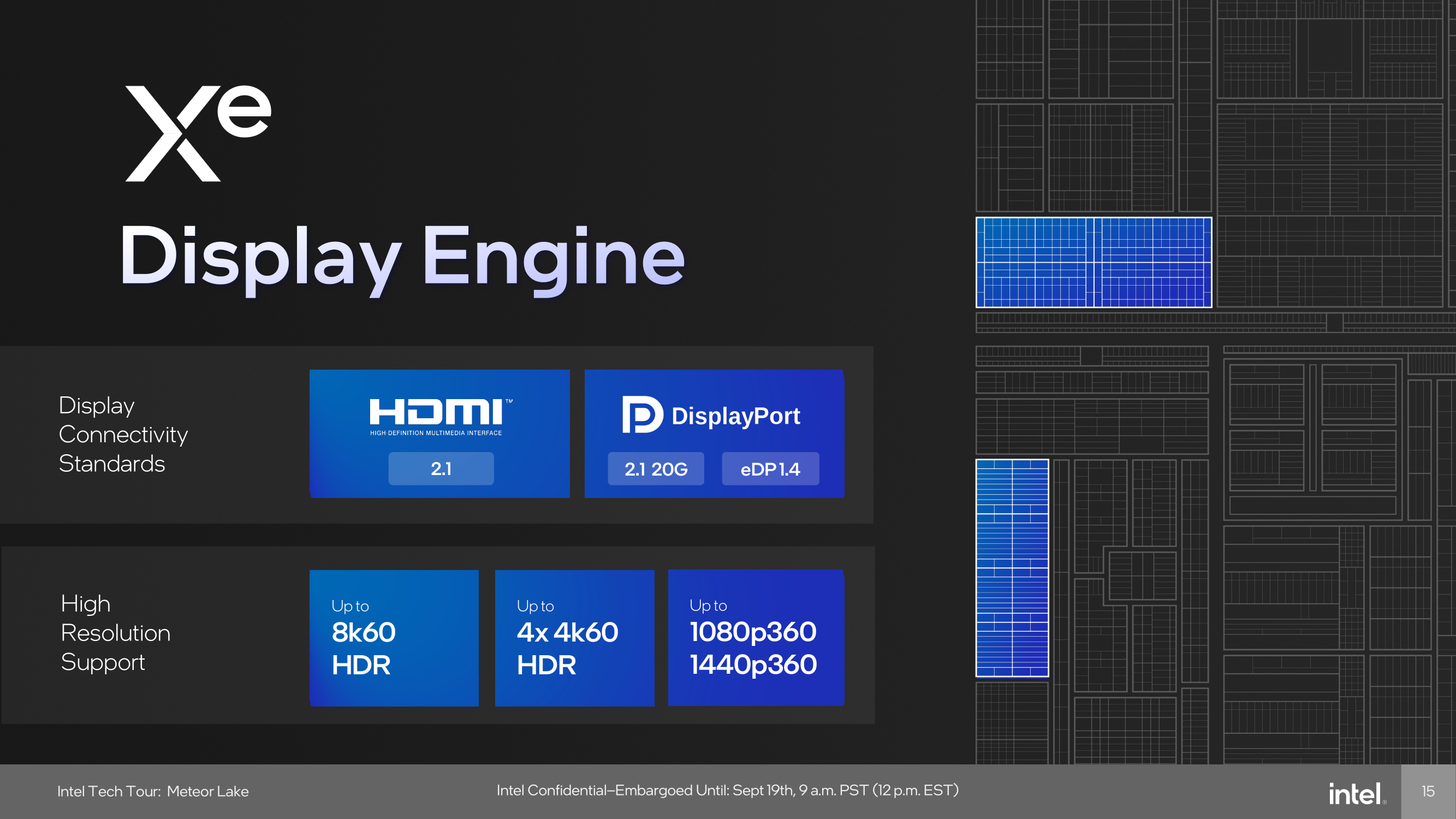
Looking at compatibility, the Xe Display Engine looks to use the latest connections and ports, including native support for HDMI 2.1, DisplayPort 2.1, Embedded DisplayPort (eDP) 1.4. and even DSC 1.2a. Via these blocks, Meteor Lake can support displays up to 8K60 HDR, or up to 4 x 4K60 HDR displays, and this is on top of 1080p360 and 1440p360 too. This gives Meteor Lake substantial display and multimedia device support, including current and up-and-coming panels.


107 Comments
View All Comments
erinadreno - Tuesday, September 19, 2023 - link
Chiplets on mobile processors doesn't sound exactly enticing. Why does Intel feel the need to use 3 different types of chiplets from 2 foundries on a power-sensitive mobile chip?jazzysoggy - Tuesday, September 19, 2023 - link
It's not the same chiplet strategy as AMD is using for Zen, it's more inline with AMD's MI accelerators. Not as cheap as the Zen strategy, but much more power efficient for power sensitive mobile chips.schujj07 - Tuesday, September 19, 2023 - link
Do you have proof it is more power efficient? Intel right now is vastly less power efficient than AMD and that is regardless of chiplet or monolithic dies.Unashamed_unoriginal_username_x86 - Tuesday, September 19, 2023 - link
First page says .15-.3 pJ/bit for Foveros, AMD has previously stated infinity fabric uses "<2 pJ/bit" which presumably isn't very far under 2. this puts Intel at 5-10x the efficiency for this very specific part of data transmissionduploxxx - Wednesday, September 20, 2023 - link
first generations of infinity fabric were also less power hungry, untill they noticed what is needed to get things faster and there you go. Lots of bandwidth changes and infinity fabric changes and as well the power usage... lets see what Intel is capable of doing first, it's marketing all over the place...Samus - Tuesday, September 19, 2023 - link
Intel is behind AMD on power efficiency purely due to process node. Architecturally they are quite competitive. This is proven in how AMD performance scales when underclocked compared to Intel.Anandtech recently did an investigation into this and came to the conclusion that while the architectures are vastly different they have potentially similar performance once you determine the ideal wattage for the chip, and at the moment Intel is pushing high TDP into extremely inefficient territory to have something competitive with AMD, due to AMD being on a superior node. Basically AMD can deliver X performance at 56w while Intel can deliver X performance at 72w, but Intel can deliver Y performance at 100w while AMD delivers Y performance at 95w.
While impossible to absolutely prove, various factors can help determine this differential has more to do with manufacturing superiority than design superiority.
Intel going for tiles here is a clear attempt to close the gap on this.
PeachNCream - Thursday, September 21, 2023 - link
I think I'd second-guess anything Anandtech does these days. They had one person with an advanced degree that departed years ago after being bought out by Qualcomm when they owned Killer NICs and have since had trouble publishing articles without obvious typos and "in-a-hurry" oversights.On the other hand, if that data is supported by a more credible publisher that has decent measuring equipment and can afford to purchase its own test hardware rather than relying solely on free samples - well then we should sit up and take notice. At this point though, an Anandtech exclusive is just a reason to raise the citation needed flag and THEN further analyze the sources for their motives.
RedGreenBlue - Sunday, October 1, 2023 - link
They’ve always had typos that slip through, or grammar mistakes. All the way back to Anand’s time. I don’t like it but I know what was intended when I see one. There still isn’t another website with the same focus on the segments they focus on. I miss the deep-dives into mobile chips and phones they used to do by investigating what wasn’t publicly released about things but for most people that’s a niche purpose that other sites cover extensively with reviews and can focus on and is a bit too consumer focused and easily found elsewhere. Not really their target market.Composite - Thursday, September 28, 2023 - link
This is indeed similar to MI250 2.5D fabric. However, MI300X is full 3D fabric.elmagio - Tuesday, September 19, 2023 - link
My personal guess, from the moment this was announced, has been that they want every single cm² of silicon going through their Intel 4/EUV capacity going to the compute tile. They're lagging quite a bit behind TSMC and Samsung in terms of EUV capacity, so anything that doesn't stand to benefit much from being designed from the ground up to be made on their own nodes is worth offloading to TSMC.SoC and IO tiles are really not process-limited currently, and their Arc GPUs are in general going manufactured elsewhere anyway. But their CPU design process has always been fully in house every step of the way, and they don't want to change that (at least not yet). So everything but compute would be "wasted" Intel 4 capacity.