Intel Unveils Meteor Lake Architecture: Intel 4 Heralds the Disaggregated Future of Mobile CPUs
by Gavin Bonshor on September 19, 2023 11:35 AM ESTSoC Tile, Part 1: Low-Power Island E-Cores, Designed for Ultimate Efficiency
Diving a little deeper into the SoC tile within Intel's Meteor Lake architecture, Intel hasn't just opted for a minor change but has made a significant leap forward, especially regarding I/O fabric scalability. The SoC tile itself isn't built on Intel 4 like the compute tile but is made by TSMC on their N6 node. Intel has ditched the old limitations of mesh routing by implementing a Network-On-Chip (NOC) on the silicon. This isn't just about making data lanes faster; it's about outlining smarter and more power-efficient access to memory. Likely an innovation from Intel's acquisition of NetSpeed back in 2018, which specialized in NoC and Fabric IP for SoCs, Intel opting for a physical NOC allows Intel to reduce the limits on bandwidth. Using EMIB and the nature of 2D scaling, the data paths are a lot shorter, translating into less power loss, but shorter wires also help reduce overall latency penalties.
Switching gears to low-power workload efficiency, Meteor Lake incorporates E-cores directly into the SoC tile, which Intel calls Low Power Island (LP) E-cores. Think of it as Intel's way of saying, "Why use a sledgehammer when a scalpel will do?". This means that the LP E-Cores are driven purely from a power-saving perspective. Having these LP E-cores available for workloads with the aid of Intel's Thread Director means lighter threads and background tasks that don't require the grunt of the P and E-cores on the compute tile can be directed onto the lower-powered LP E-cores.
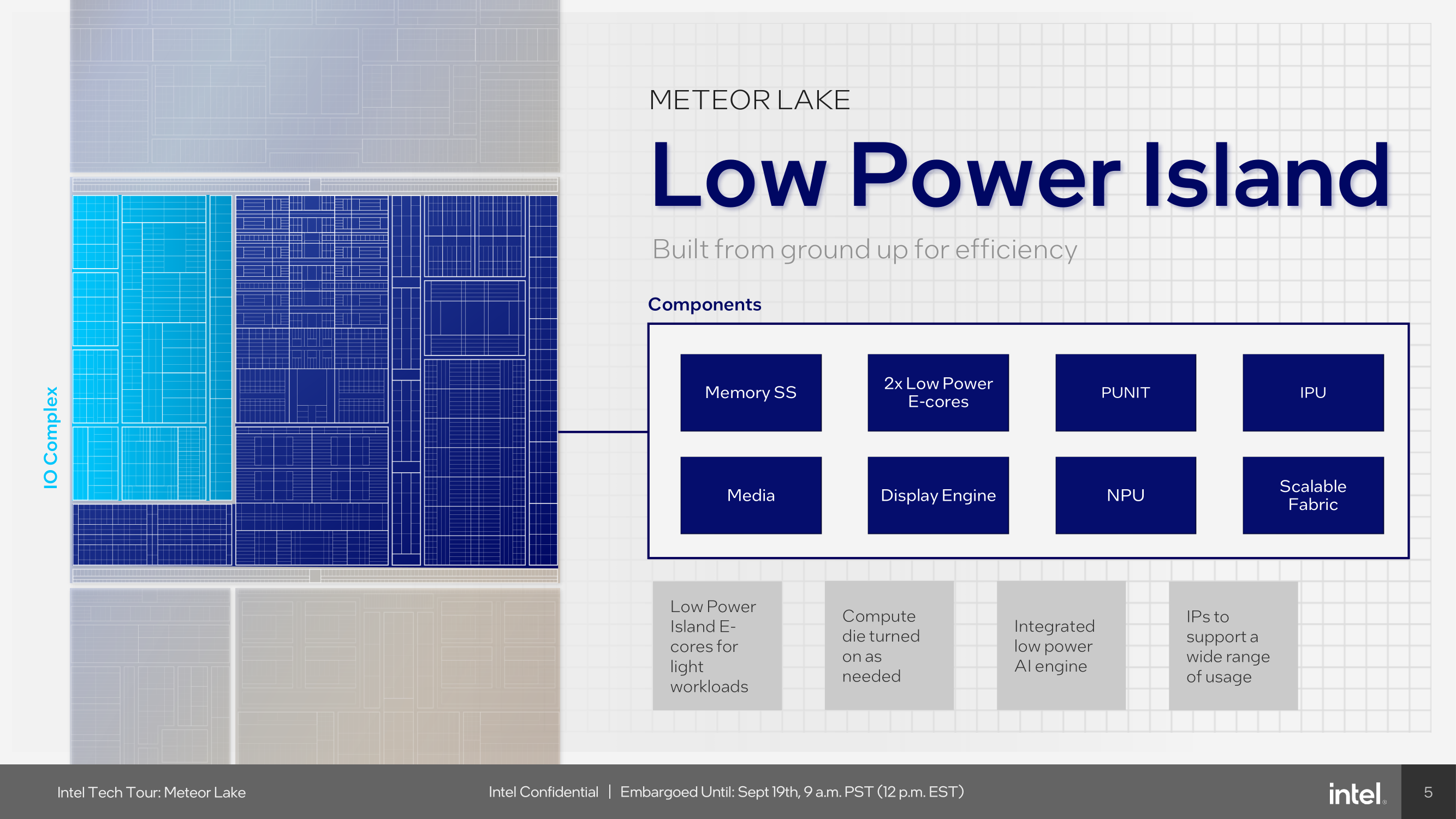
While both the E and LP E-cores are based on the same Crestmont microarchitecture, the E-cores on the compute tile are built on Intel 4, along with the P-cores. The LP E-cores are made on TSMC's N6 node, like the rest of the SoC tile. These low-power island E-cores are tuned for finer-grained voltage control through an integrated Digital Linear Voltage Regulator (DLVR), and they also have a lower voltage-to-frequency (V/F) curve than the big E-cores on the compute tile, meaning they can operate with a lower power cost, thus saving power when transitioning low-intensity workloads off of the compute tile and onto the LP E-cores.
Part of the disaggregated nature of Foveros combined with individual power management controllers (PMC) within each tile means that IP blocks can be independently powered on or off when required.
SoC Tile: Bandwidth Scalability, Can't Stop The NOC
So adding a variety of tiles requires a highly competent pathing to ensure bandwidth is adequately structured. As I/O bandwidth bottlenecking was a major concern in previous iterations, Intel aims to solve bandwidth flow restrictions with a couple of solutions.
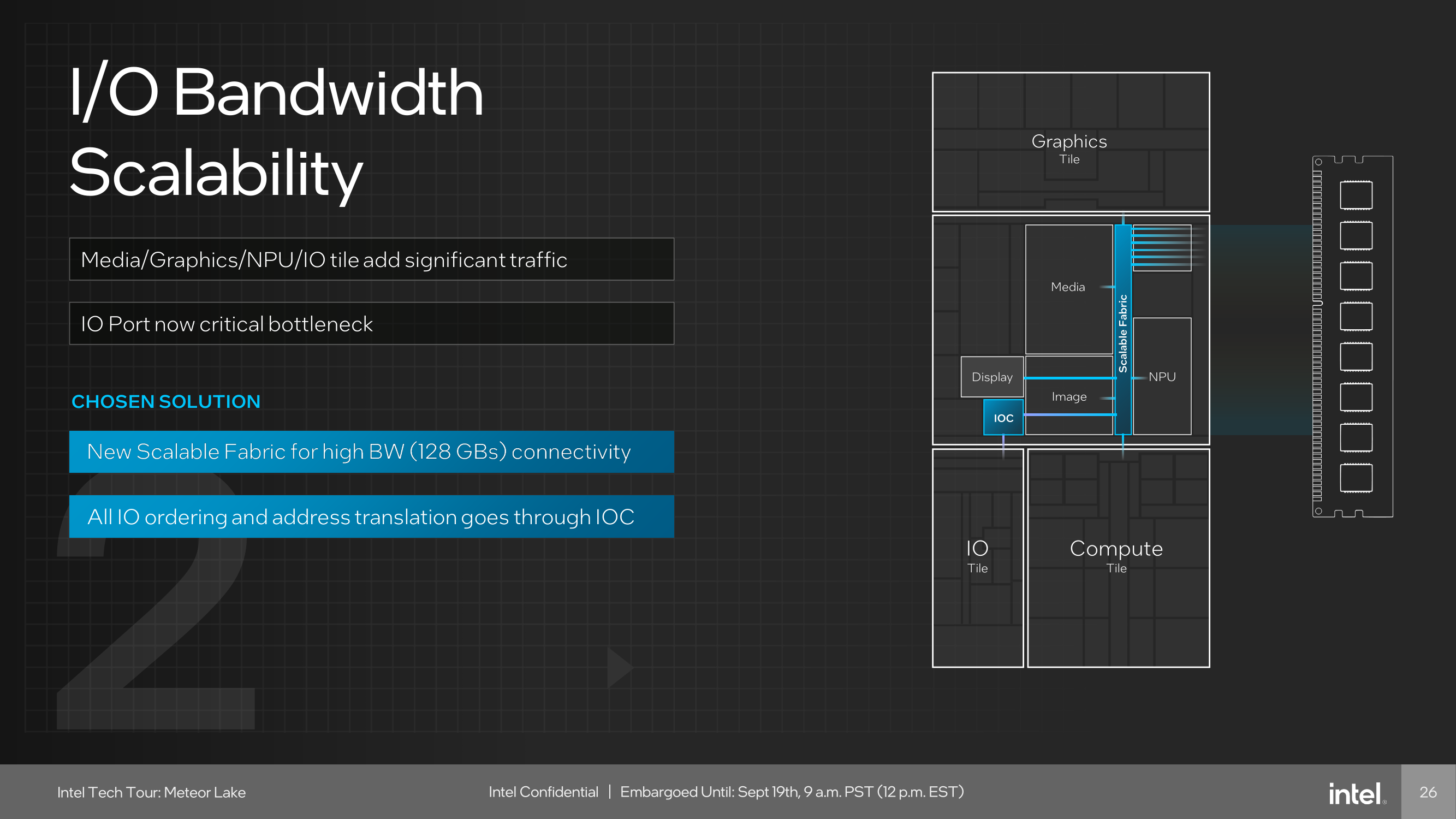
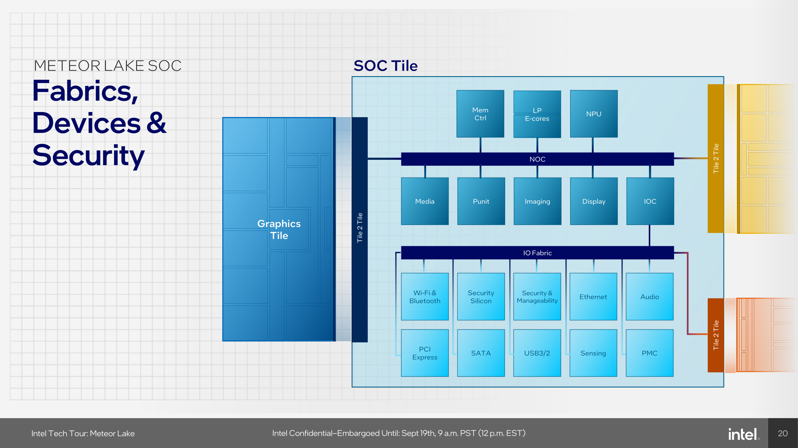
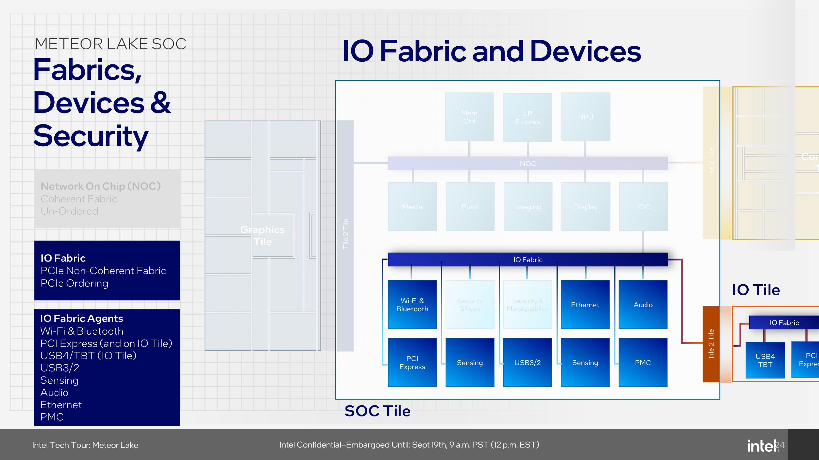
The first is through the scalability of the I/O bandwidth, which Intel does by adding what it calls 'Scalable Fabric,' which is configured for up to 128 GB/s of bandwidth throughput. All of the I/O ordering and address translation is fed through the IOC, while Intel has implanted a Network-on-Chip (NOC) to interconnect many of the different areas of the SoC.
The Network-on-Chip or NOC is designed to be coherent, and for Meteor Lake on Intel 4, this uses unordered processing, which moves data in an unordered fashion. Connecting all the tiles together through the NOC and independently through the IOC gives plenty of bandwidth headroom for devices or agents requiring it. The NOC is directly connected to the compute and graphics tile, while other elements, including the traffic fed directly through the LP E-cores on the SoC tile, media, display, the NPU, and the imaging processing unit (IPU), all going through the NOC. In terms of the connection to the I/O tile, this is connected directly to the IO fabric and then is fed through the IOC, which then goes directly to the NOC.
The SoC tile also integrates Wi-Fi 6E and can be made to support the latest Wi-Fi 7 standard. Having a future-proof method of including Wi-Fi 7 and Bluetooth 5.4 can add the next level of wireless connectivity to Intel's mobile platform. Wi-Fi 7 offers 320 MHz of bandwidth, doubling the channel width compared to its predecessor, Wi-Fi 6. It also uses 4096-QAM (4K QAM) to enable transmission speeds capable of hitting 5.8 Gbps.
We're still waiting for clarification on what this actually means. Whether it's supportive of Wi-Fi 7 or if there's some underlying compatibility within the Wi-Fi MAC integrated into the silicon. One option could be that Intel is adding a full external controller into the silicon to get to Wi-Fi 7 instead of CNVio splitting up parts of the radio stack. We have asked Intel for more details and will update you when we have a response.
That being said, Intel discloses 'support' for Wi-Fi 7 and BT 5.4, but there's a chance Intel could differentiate which wireless MAC is implemented into different chip segments. An example would be an Intel 9 Ultra SKU, bolstered by Wi-Fi 7 support, whereas a lower-end SKU like a Core 3 might utilize Wi-Fi 6E to save on cost.
Additional features include Multi-Resource Unit (RU) Puncturing and Military-grade security with WPA3 that supports GCMP-256 encryption to ensure both speed and security when connected to a wireless network. Unique features like Multi-Link Operation (MLO) in Wi-Fi 7 are designed to reduce latency and jitter by up to 60%, making it a competent solution for various user's connectivity needs. Adding Bluetooth 5.4 further complements this by improving audio quality, and it is claimed to offer up to 50% lower power consumption for longer battery life.
Also present on the SoC tile is the display controller and the media engine from the GPU. These are always-on (or at least, mostly-on) blocks that do not need to be built on a cutting-edge process node, making them good candidates to place on the SoC tile. Meteor Lake offers support for 8K HDR and AV1 video playback and contains native HDMI 2.1 and DisplayPort 2.1 connectivity.
Finally, the SoC tile also includes other key platform components, such as PCIe lanes, which are integral for connectivity to external devices such as discrete graphics cards and the platform's I/O capabilities, such as USB 4 and 3, as well as offering a direct interconnect to a separate I/O tile with Thunderbolt 4 and additional PCIe lanes. While we've touched on wireless connectivity, the SoC tiler also includes Ethernet support, although Intel hasn't disclosed yet which PHY will be included; it is likely to be capable of 2.5 GbE at the minimum.
A Note on Meteor Lake's Security Features: New Silicon Security Engine (ISSE)
Security has also been given closer attention in Meteor Lake. The architecture introduces the Intel Silicon Security Engine (ISSE), a dedicated component focused solely on securing things at a silicon level. Various vulnerabilities have been at the forefront of media over the last few years, including Meltdown, Spectre, and Foreshadow.
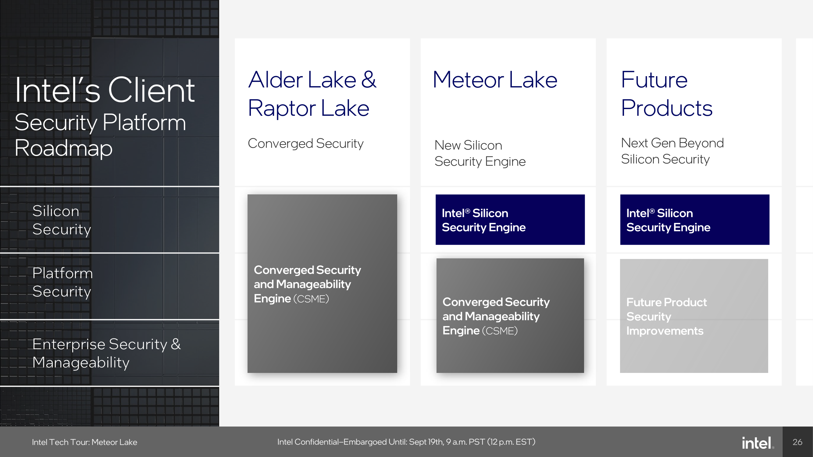
With real threats around the world, securing data is ever prevalent, and CPU architects and designers not only need to consider performance and efficiency, but security and doing some architecturally is just as important as a competent software stack. The Converged Security and Manageability Engine (CSME) has also been partitioned to further enhance platform security. These features collectively work to give a wide range of on-chip and off-chip securities designed to mitigate attacks on multiple fronts.


107 Comments
View All Comments
erinadreno - Tuesday, September 19, 2023 - link
Chiplets on mobile processors doesn't sound exactly enticing. Why does Intel feel the need to use 3 different types of chiplets from 2 foundries on a power-sensitive mobile chip?jazzysoggy - Tuesday, September 19, 2023 - link
It's not the same chiplet strategy as AMD is using for Zen, it's more inline with AMD's MI accelerators. Not as cheap as the Zen strategy, but much more power efficient for power sensitive mobile chips.schujj07 - Tuesday, September 19, 2023 - link
Do you have proof it is more power efficient? Intel right now is vastly less power efficient than AMD and that is regardless of chiplet or monolithic dies.Unashamed_unoriginal_username_x86 - Tuesday, September 19, 2023 - link
First page says .15-.3 pJ/bit for Foveros, AMD has previously stated infinity fabric uses "<2 pJ/bit" which presumably isn't very far under 2. this puts Intel at 5-10x the efficiency for this very specific part of data transmissionduploxxx - Wednesday, September 20, 2023 - link
first generations of infinity fabric were also less power hungry, untill they noticed what is needed to get things faster and there you go. Lots of bandwidth changes and infinity fabric changes and as well the power usage... lets see what Intel is capable of doing first, it's marketing all over the place...Samus - Tuesday, September 19, 2023 - link
Intel is behind AMD on power efficiency purely due to process node. Architecturally they are quite competitive. This is proven in how AMD performance scales when underclocked compared to Intel.Anandtech recently did an investigation into this and came to the conclusion that while the architectures are vastly different they have potentially similar performance once you determine the ideal wattage for the chip, and at the moment Intel is pushing high TDP into extremely inefficient territory to have something competitive with AMD, due to AMD being on a superior node. Basically AMD can deliver X performance at 56w while Intel can deliver X performance at 72w, but Intel can deliver Y performance at 100w while AMD delivers Y performance at 95w.
While impossible to absolutely prove, various factors can help determine this differential has more to do with manufacturing superiority than design superiority.
Intel going for tiles here is a clear attempt to close the gap on this.
PeachNCream - Thursday, September 21, 2023 - link
I think I'd second-guess anything Anandtech does these days. They had one person with an advanced degree that departed years ago after being bought out by Qualcomm when they owned Killer NICs and have since had trouble publishing articles without obvious typos and "in-a-hurry" oversights.On the other hand, if that data is supported by a more credible publisher that has decent measuring equipment and can afford to purchase its own test hardware rather than relying solely on free samples - well then we should sit up and take notice. At this point though, an Anandtech exclusive is just a reason to raise the citation needed flag and THEN further analyze the sources for their motives.
RedGreenBlue - Sunday, October 1, 2023 - link
They’ve always had typos that slip through, or grammar mistakes. All the way back to Anand’s time. I don’t like it but I know what was intended when I see one. There still isn’t another website with the same focus on the segments they focus on. I miss the deep-dives into mobile chips and phones they used to do by investigating what wasn’t publicly released about things but for most people that’s a niche purpose that other sites cover extensively with reviews and can focus on and is a bit too consumer focused and easily found elsewhere. Not really their target market.Composite - Thursday, September 28, 2023 - link
This is indeed similar to MI250 2.5D fabric. However, MI300X is full 3D fabric.elmagio - Tuesday, September 19, 2023 - link
My personal guess, from the moment this was announced, has been that they want every single cm² of silicon going through their Intel 4/EUV capacity going to the compute tile. They're lagging quite a bit behind TSMC and Samsung in terms of EUV capacity, so anything that doesn't stand to benefit much from being designed from the ground up to be made on their own nodes is worth offloading to TSMC.SoC and IO tiles are really not process-limited currently, and their Arc GPUs are in general going manufactured elsewhere anyway. But their CPU design process has always been fully in house every step of the way, and they don't want to change that (at least not yet). So everything but compute would be "wasted" Intel 4 capacity.