FIRST LOOK: ULi M1697 for Athlon 64/x2
by Wesley Fink on December 13, 2005 12:05 AM EST- Posted in
- CPUs
Basic Features: ULi M1697 Single Chip
The ULi Award BIOS provides a typical range of BIOS control options for a Reference Board used to qualify a chipset. The wide 200 to 400 range for CPU clock was a pleasant surprise, but it is somewhat academic with no memory voltage controls present in the BIOS. The memory tweaking adjustments were extensive, but of limited use without some means of controlling memory voltage. Reference Boards demonstrate chipset features and capabilities to manufacturers, and ULi clearly shows that the M1697 is capable of supporting whatever range of BIOS control or Voltage control features that the manufacturer might wish to implement.
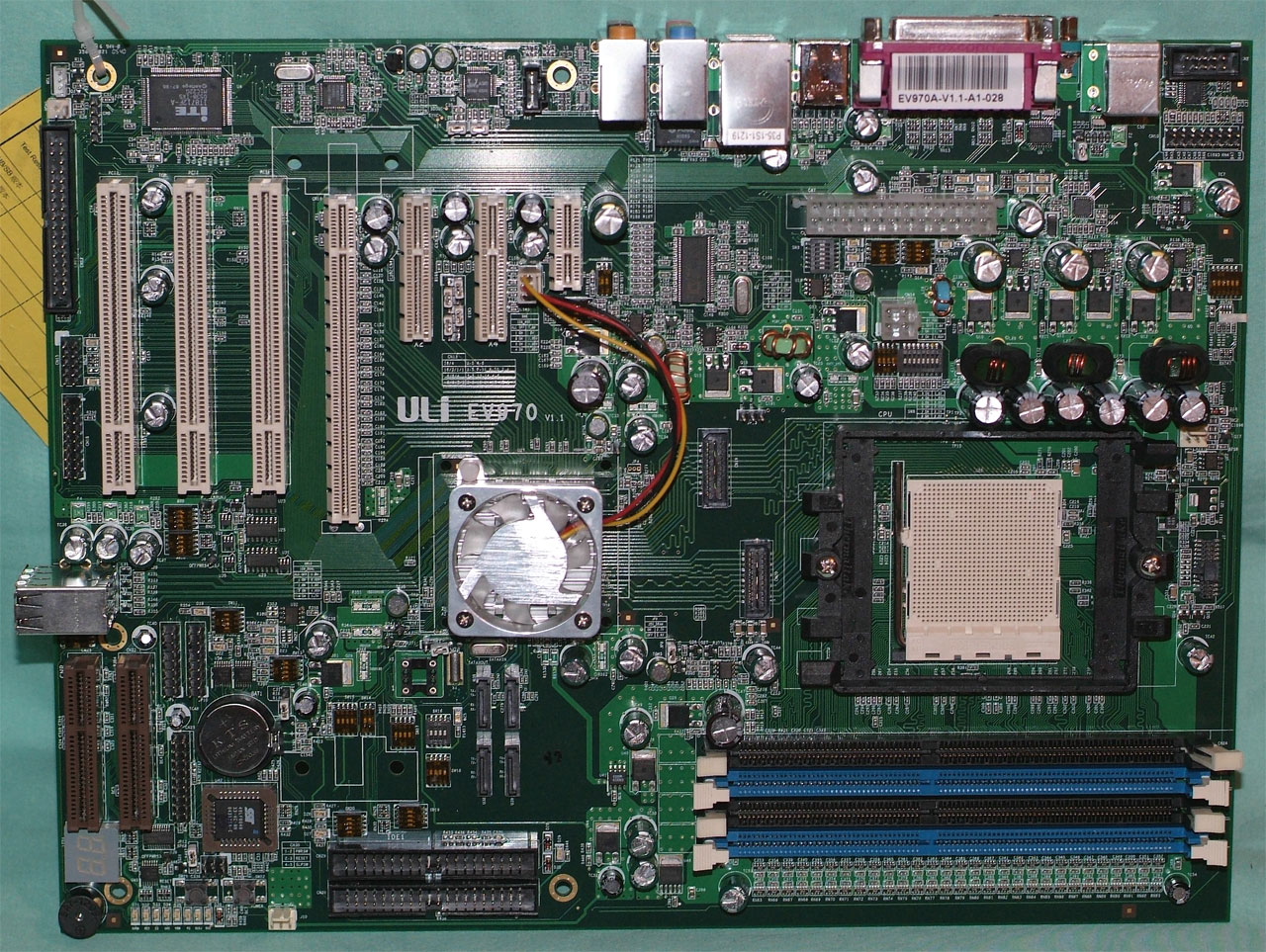
The location of the floppy connector at the bottom of the board will be a long reach for floppy users. Many buyers don’t care about floppies any more, but if you still use them, the bottom of the board is an inconvenient and hard to reach location.
| ULi M1697 | |
| CPU Interface | Socket 939 Athlon 64 |
| Chipset | ULi M1697 Single-Chip |
| Bus Speeds | 200 to 400MHz in 1MHz Increments |
| PCIe Speeds | 100-125MHz in 1MHz Increments |
| PCI/AGP | Fixed at 33/66 |
| AMD K8 Cool'n'Quiet | Auto, Disable |
| Core Voltage | Startup, 0.825V to 1.55V in 0.025V increments |
| CPU Clock Multiplier | Startup, 4x-25x in 1X increments |
| HyperTransport Frequency | 1000MHz (1GHz) |
| HyperTransport Multiplier | 200, 400, 600, 800, 1000, Auto |
| DRAM Voltage | Provision for 2.62V, 2.72V (Not implemented) |
| HyperTransport Voltage | 1.20, 1.25, 1.30, 1.35, 1.40V by DIP Switch |
| Chipset Voltage | 1.80 to 2.2V in .05V increments by DIP Switch |
| PCIe Voltage | 1.80 to 2.0V in .05V increments by DIP Switch |
| M1697 Resume Power | 1.70, 1.80, 1.85, 1.90, 2.02V by DIP Switch |
| Memory Slots | Four 184-pin DDR DIMM Slots Dual-Channel Configuration Regular Unbuffered Memory to 4GB Total |
| Expansion Slots | 1 PCIe x16 (or 2 PCIe x8) 1 x1 PCIe 1 x2 PCIe 1 x4 PCIe 3 PCI Slots 1 CNR Slot 1 LPC slot |
| Onboard SATA/RAID | 4 SATA2 3Gb/s Drives by ULi M1597 (RAID 0,1,0+1,5,JBOD) |
| Onboard IDE/IDE RAID | Two Standard ATA133/100/66 (4 drives) |
| Onboard USB 2.0/IEEE-1394 | 8 USB 2.0 ports supported by ULi M1597 No Firewire (Optional) |
| Onboard LAN | 10/100 Ethernet by Realtek PNY |
| Onboard Audio | HD Azalia 7.1 by Realtek ALC883 |
| BIOS Revision | Award OCAP1130 Evaluation ROM |
The ULi Award BIOS provides a typical range of BIOS control options for a Reference Board used to qualify a chipset. The wide 200 to 400 range for CPU clock was a pleasant surprise, but it is somewhat academic with no memory voltage controls present in the BIOS. The memory tweaking adjustments were extensive, but of limited use without some means of controlling memory voltage. Reference Boards demonstrate chipset features and capabilities to manufacturers, and ULi clearly shows that the M1697 is capable of supporting whatever range of BIOS control or Voltage control features that the manufacturer might wish to implement.
Click to enlarge.
The location of the floppy connector at the bottom of the board will be a long reach for floppy users. Many buyers don’t care about floppies any more, but if you still use them, the bottom of the board is an inconvenient and hard to reach location.


51 Comments
View All Comments
Wesley Fink - Wednesday, December 14, 2005 - link
The AMD on-chip memory controller does NOT support Cammand Rate 2 timings with 4 dimms, and yet the DFI RDX200 motherboard is able to run four double-sided dimms at 2-2-2 at 1T Command Rate due to clever BIOS engineering. The early AMD controllers stated that 4 dimms must run at DDR400 at slower timings or drop to DDR333 for fastest timings, and yet almost every top motherboard we tested found ways to run 4 dimms at the fastest memory timings. Some of the boards could not do this with the exact same processor - Epox is an example that comes to mind.The point is, we well understand the architecture of the AMD processor and memory controller, but you are seriously mistaken if you think the chipset and BIOS do not affect memory timings and performance on an AMD motherboard. The impact is much less than on Intel motherboards with the memory controller in the chipset, but the chipset and BIOS DO impact memory compatibility and performance on AMD boards. We have proven that over time with many tests with the same CPU (and therefore the same memory controller).
Peter - Thursday, December 15, 2005 - link
The chipset does not have an influence on RAM. I am not mistaken. The only connection between RAM and chipset is the SMbus channel that lets the BIOS read out the SPD EEPROM from the DIMM - but the entire operational bus for the RAM traffic is connected to the CPU and nowhere else.The board layout of course does have an influence, and so does the amount of fine tuning done in this particular board's BIOS. Being a BIOS engineer sitting right in the middle of mainboard engineering, I sure know that. Besides, "clever BIOS engineering" cannot magically make things possible that physically aren't - so if you want tight timings, you better come up with a damn good mainboard routing job.
Still, I see this as an attempt at deceiving from what your article said. There, you are attributing RAM operation to the chipset in several places. This is all wrong, and has been all wrong in every single AMD64 chipset review Anandtech ever made. Get over it, skip this cut&paste section unless you're doing a P4 chipset review.
So you meant to be testing board layout limits? On a pure reference board, we might find this to be rather pointless - and if it's an available product, you still need to get the description corrected. You are NOT testing chipset capabilities when you are poking around the RAM on an AMD64.
btw, the AMD on-chip memory controller does support 2T command rate. It is the official JEDEC PC3200 standard that does not officially support two DIMMs per channel at 200 MHz. All that AMD did in later revisions is increase the headroom above what's SUPPOSED to work. The very first Athlon64 was spot on JEDEC specifications, nothing to complain about there either. One DIMM at 200 MHz, two at 333, three at 266. Everything (!) above that is YMMV territory.
Wesley Fink - Monday, December 19, 2005 - link
There are numerous DFI BIOS for the DFI nF4 boards that are customized for best performance with various RAM. Board layout does matter a great deal, but if only the memory controller or board layout mattered in AMD RAM performance these BIOS revisions for the same board would have no impact at all. It appears you are certain you are a much more capable "BIOS Engineer" than Oskar Wu or many others I have talked with who definitely disagree with your conclusions. We all understand your point, which is basically correct, but that is not the end of the story or even close to the complete story.You are correct in your truths, and it is not likely you will be dissuaded with facts that contradict your conclusions. NO ONE at AT is trying to deceive anyone.
Peter - Tuesday, December 20, 2005 - link
I'm referring to the following statements on page 4, and I'm certain the honorable Mr. Wu would know better than writing things like:>Memory Stress Testing: Since this is a new chipset, the best setting for tRAS was first determined.
>This means that any setting from 6 to 11 tRAS will work well with this chipset.
>*7T was determined by MemTest86 benchmarks to deliver the widest bandwidth with the ULi M1697 chipset.
(my highlighting)
These statements all directly attribute RAM performance to the ULi chipset, which we all know is plain wrong.
The fact that the board's layout has an influence is not what I'm disputing. Of course it does. BIOS fine tuning can only get the most out of that given hardware layout, no magic there, just patience and persistance - and then there's the great moving target of DIMM behavior that provides for a nice murky cloud of guesstimation between stability and performance - that's why BIOS updates are frequently seen. This I'm not disputing either, after all that's exactly what I'm doing (only that I'm working on DIMM-less platforms where you don't have to deal with that aspect, only the board's own layout and the differences in the actual RAM _chips_).
But these are all distractions that you muddied the waters with. The original point of my posting, and the only complaint I have, is:
You're failing to acknowledge - and subsequently failing to represent correctly in your articles about AMD64 mainboards and chipsets - is that the chipset isn't involved in this AT ALL.
Get it right. Please.
ocyl - Tuesday, December 13, 2005 - link
I wished that this article had talked about the disliked DRM component of this chipset...Alphafox78 - Tuesday, December 13, 2005 - link
Did anyone else notice that the CPU in the diagram is a K5?! hahLonyo - Tuesday, December 13, 2005 - link
It would be nice if you had overclocked, just to give a orugh idea of what the chipset was capable of.In case you weren't aware, there is a nice OCZ booster which increases memory voltage where such options may be unavailable, so maybe in future you could think of using this, just to give a rough idea of overclocking potential. (Assuming it works).
Wesley Fink - Tuesday, December 13, 2005 - link
Reviews of Reference Boards have been criticized by some readers in the past for testing overclocking capabilities "on a board no one can actually buy". Our position has been to test OC on Reference Boards where it is possible - to give a rough idea, as you put it, of OC capabilities.However, a board that does not even implement any memory voltage controls is not likely to be representative of a chipset's OC capabilities. We have been promised production boards very soon and we will defintely test OC on those. Yes, we have an OCZ RAM Booster in the lab.
Creig - Tuesday, December 13, 2005 - link
There's no doubt that the ASRock 939Dual-SATA2 has been an extremely popular board, but it could be improved upon. Apparently ASRock is considering doing just that. The ULi M1697 can be paired with the M1695 on one motherboard to create a board with two 16x PCI-E, AGP, SATA-II, HD audio and a better range of CPU/DIMM voltages.http://www.ocworkbench.com/ocwbcgi/ultimatebb.cgi?...">http://www.ocworkbench.com/ocwbcgi/ulti...bb.cgi?u...
Looks like ULi/ASRock are on a roll.
psychobriggsy - Tuesday, December 13, 2005 - link
Hmm, not having Gigabit might affect, err, a few people. The vast majority will have 100mbit home networks however, and thus not having gigabit isn't an issue. In the corporate area it may be an issue, but they'd probably prefer a standard gigabit controller than a built-in one anyway, so having one run off PCIe isn't an issue.The chipset looks pretty good though, nice feature set. Hope it does well.