TSMC Outlines 2nm Plans: N2P Brings Backside Power Delivery in 2026, N2X Added To Roadmap
by Anton Shilov on April 26, 2023 3:10 PM EST
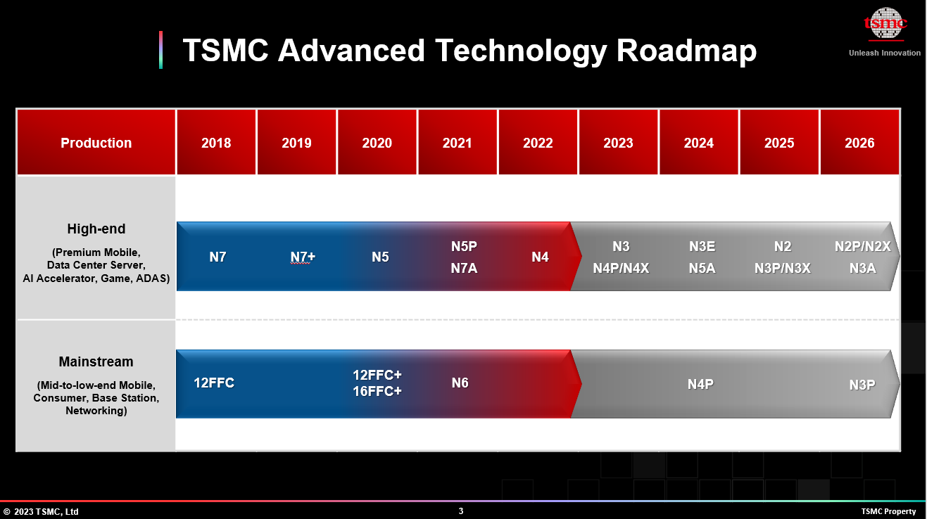
At its 2023 North American Technology Symposium today, TSMC has disclosed additional details about its plans for its forthcoming N2 2nm-class production nodes in 2025 – 2026 and beyond. TSMC's N2 family of fabrication technologies will be expanding with additional variations, including N2P with backside power delivery, and N2X for high-performance computing. Between these forthcoming N2 generation process nodes, TSMC is laying out a roadmap to continue their relentless pace of increasing transistor performance efficiency, optimize power consumption, and improving transistor density.
N2 Gets Denser
TSMC's initial N2 manufacturing process, which was introduced last year, will be the foundry's first node to use gate-all-around (GAAFET) transistors, which TSMC is calling Nanosheet transistors. GAAFET's advantages over current FinFET transistors includes lowered leakage current (as gates are present on all four sides of the channel), as well as the ability to adjust channel width for higher performance or lower power consumption.
When introducing this technology last year, TSMC said that it would enhance transistor performance by 10% to 15% with the same power and complexity, or reduce power consumption by 25% to 30% at the same clock and transistor count. The company also says that N2 will offer 'mixed' chip densities of over 15% greater than N3E, which is an increase from the 10% density increase announced last year.
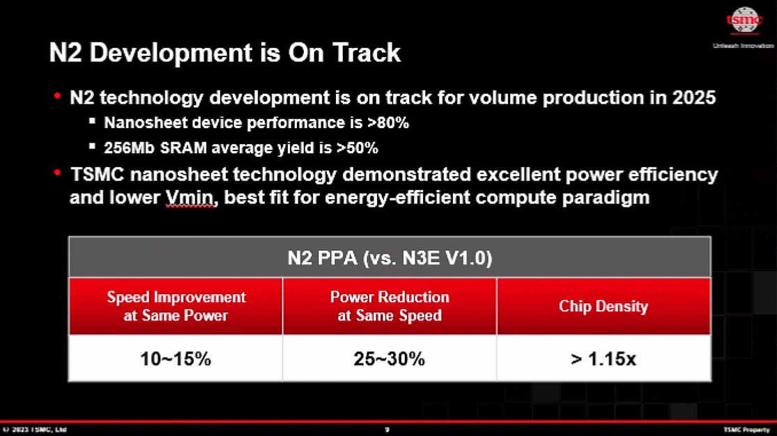
Today, the company said that N2 technology development is on track and the node will enter high-volume production in 2025 (probably very late 2025). The company also said that its Nanosheet GAA transistor performance is achieving better than 80% of its target specifications two years before entering HVM, and that average yield of a 256Mb SRAM test IC is over 50%.
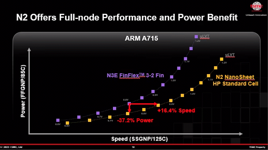
"TSMC nanosheet technology demonstrated excellent power efficiency and lower Vmin, best fit for energy-efficient compute paradigm," a statement by TSMC reads.
| Advertised PPA Improvements of New Process Technologies Data announced during conference calls, events, press briefings and press releases |
|||||
| TSMC | |||||
| N5 vs N7 |
N3 vs N5 |
N3E vs N5 |
N2 vs N3E |
||
| Power | -30% | -25-30% | -34% | -25-30% | |
| Performance | +15% | +10-15% | +18% | +10-15% | |
| Chip Density* | ? | ? | ~1.3X | >1.15X | |
| Volume Manufacturing |
Q2 2022 | H2 2022 | Q2/Q3 2023 | H2 2025 | |
*Chip density published by TSMC reflects 'mixed' chip density consisting of 50% logic, 30% SRAM, and 20% analog.
N2P Gets Backside Power Delivery In 2026
TSMC's N2 family will evolve and sometime in 2026, when the company plans to introduce its N2P fabrication technology. N2P that will add backside power rails to N2's Nanosheet GAA transistors.
Backside power delivery is meant to decouple I/O and power wiring by moving power rails to the back, addressing challenges like elevated via resistances in the back-end-of-line (BEOL). This, in turn, will enhance transistor performance and reduce their power consumption. Also, backside power deliver eliminates some potential interference between data and power connections.
Backside power delivery is innovation whose importance is hard to overstate. Chipmakers have been fighting resistances in chip power delivery circuitry for years, and backside power delivery networks (PDN) are a yet another method to address them. In addition, decoupling PDN and data connections also helps with area reduction, so expect N2P to further increase transistor density compared to N2.
For now, TSMC is not disclosing any hard numbers regarding N2P's performance, power, and area (PPA) advantages over N2. But based on what we hear from industry sources, backside power rails alone could bring a single digit power improvements and double-digit transistor density improvements.
TSMC says that N2P is on track to be production ready in 2026, so we can speculate that the first N2P-based chips will be available in 2027. This timeline would put TSMC roughly two years behind rival Intel when it comes to backside power, assuming they're able to ship their own 20A process on time in 2024.
N2X: Even More Performance
In addition to N2P, which will likely be a working horse of TSMC's 2nm generation of processes, TSMC is also prepping N2X. This will be a fabrication process tailored for high-performance computing (HPC) applications like high-end CPUs, which need increased voltages and clocks. The foundry is not outlining the specific advantages this node will compared to N2, N2P, and N3X, but as with all performance-enhanced nodes, the actual benefits are expected to depend signficantly on how much design technology co-optimization (DTCO) is practiced.


38 Comments
View All Comments
dotjaz - Thursday, April 27, 2023 - link
And if TSMC's official figure is to be believed, it's also less than 3.6% better than N4P. Further proof of density no longer bring performance.N2 is on the same boat. Moderate density increase gives notable performance boost, and yes 10~15% IS notable for one generation. I don't know what you expect. N3E is only 3~7% better than N3, N3 is only -1~3.6% better than N4P.
Ryan Smith - Thursday, April 27, 2023 - link
N2 is not intended to bring a big density increase. Its big feature is the switch to much better performing nanosheet (GAAFET) transistors.lemurbutton - Thursday, April 27, 2023 - link
If it's better performing, why isn't it reflected in the performance increase numbers? It's still "+10-15%" vs N3E.
techjunkie123 - Thursday, April 27, 2023 - link
+10-15% perf or -25-30% power is basically a full node improvements worth of benefit. See the numbers for N3 vs N5 or previous numbers for N5 vs N7. But in the case of N2 the performance improvements are not accompanied by density improvements.caribbeanblue - Friday, May 5, 2023 - link
Yes you’re right, on paper the improvement of 3nm looks similar to previous gen process nodes, however you’re ignoring another variable that should be considered in the equation, which is the price. On previous generation nodes, yes you reaped similar benefits as the 3nm node, but the node was also a similar price or cheaper compared to the previous node in that you could keep the die size the same, so instead of sticking with the same chip design as last year and just shrinking it and making it cheaper, chip designers could amplify the benefits of the new process node by adding in wider designs. But now with 3nm, the price increase is almost as much if not higher than the density increase, meaning new chips are going to have to stick with pretty much the existing transistor layout besides tweaking it a little bit to port it over to the new node, and only get the raw process node benefits, such as 15% higher freq. or 35% less power draw. Whereas on 7nm or 10nm, you would get that 15% higher frequency, but a wider design afforded by having the luxury of keeping the die size similar gave you that much more performance on top of that.dotjaz - Thursday, April 27, 2023 - link
What are you on about? +10-15% isn't 0%. How is it not better performing?FinFET is at the end of the road. It's no longer economically viable to increase performance on FinFET.
lemurbutton - Friday, April 28, 2023 - link
Previous node improvements included +10-15% increase in performance and 1.6 - 1.7x increase in density.This node only adds 1.15x increase in density and the same performance increase.
That's my point.
AzureNeptune - Saturday, April 29, 2023 - link
You're comparing apples to oranges. The 1.15x number is for "chip density", which as stated in the article is mixed density of logic, SRAM, and analog. Huge density increases like 1.7x for N3 were only for logic. SRAM and analog are hardly scaling (or not at all). Obviously N2 won't have 1.7x logic but it'll probably be something like 1.4-1.5x which for also introducing GAA is not bad.lemurbutton - Tuesday, May 2, 2023 - link
N5 to N3E is double the density of N3E to N2. No matter how you slice it, N2 seems like a weak full node upgrade based on what we know so far.name99 - Thursday, April 27, 2023 - link
The primary constraint on density right now (even for N3) is wiring. Smaller transistors are nice for power/performance reasons, but you can't pack them closer together than wiring allows.BSPD will improve this situation substantially. BUT there are multiple different ways to implement BSPD. Some are focussed primarily on reducing the voltage drop of power delivery; some also care a lot about alleviating wiring congestion.
The three basic BSPD schemes are described here: https://www.fabricatedknowledge.com/p/backside-pow...
TSMC, in their usual way, seems to be approaching the problem by implementing the simplest solution first, presumably with a schedule to update the scheme one year at a time (so an N2+ or NA18 or whatever that switches to a Power Via type scheme, then maybe an NA16 that uses Backside Contacts). Intel believe they can bypass learning by doing and just jump straight to Power Via. These sorts of long distance leaps have worked out spectacularly badly for Intel (and then Samsung) over the past decade so I can't understand what makes them think this time will be different, but whatever, that's the way this lines up:
- TSMC pretty much guaranteed to work in 26, to work better in 27, to work best of all in 28
- INTC claiming to be at level "better" in 2024Q3 with the all important caveat "Ramp/Retail may vary"...