Arm Announces Neoverse V1, N2 Platforms & CPUs, CMN-700 Mesh: More Performance, More Cores, More Flexibility
by Andrei Frumusanu on April 27, 2021 9:00 AM EST- Posted in
- CPUs
- Arm
- Servers
- Infrastructure
- Neoverse N1
- Neoverse V1
- Neoverse N2
- CMN-700
The CMN-700 Mesh Network - Bigger, More Flexible
It’s been a whole 5 years since we last wrote about Arm’s Coherent Mesh Network, the current generation CMN-600. The IP was announced quite some time ago, but has been a mainstay of Arm’s infrastructure IP for some time now, with it seeing some iterations in terms of IP revisions, with r2 introducing some important changes such as larger caches and CCIX capability.
Along with the V1 and N2, Arm today is also announcing a new generation CMN product in the form of the new CMN-700, promising much larger improvements to how Arm’s mesh network operates and what it is capable of in terms of scalability, performance, and flexibility.
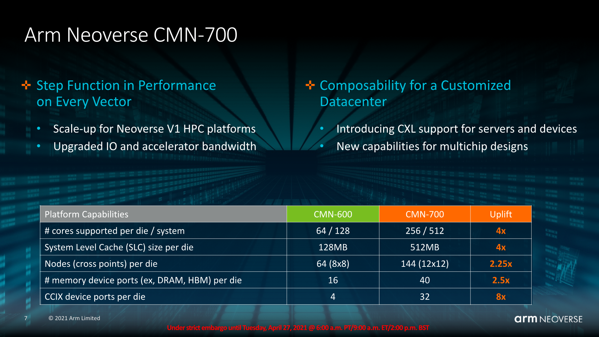
Starting off with the basic characteristics of the new design, the important big new feature is the fact that the mesh now has grown from a limit of 8 x 8 nodes (64) to 12 x 12 (144), allowing Arm to increase the number of CPUs on a single mesh and silicon die.
Terminology:
- RN-F: Fully coherent Request Node – Typically a CPU core, a CAL with two cores, or a DSU cluster
- HN-F: Fully coherent Home Node – A block of SLC cache with Snoop Filter
- CAL: Component Aggregation Layer – A block that houses two CPU cores connecting to one RN-F port
The actual maximum number of cores in a mesh has grown from 64 to 256, the latter number achievable through 128 RN-F request nodes each with 2 cores through a CAL (Component Aggregation Layer). For attentive readers, it might be weird to see Arm say that the CMN-600 only supports up to 64 cores when we have 80-core designs such as the Altra out there. Arm explained that the 64-core limit is through native cores connected to RN-F’s or through CALs, and that it’s actually possible to host more cores when you integrate them into the mesh through DSU (DynamiQ Shared Units). Ampere never confirmed their mesh layout, but this seems to be the only explanation of how they’d achieve a core count that high on the CMN-600.
Alongside 128 RN-Fs, hosting up to 256 cores, the chip hosts up to 128 HN-F home nodes, meaning nodes in which the SLC (System Level Cache) resides. Arm here discloses a maximum SLC of up to 512MB per die, meaning 4MB per node, while oddly enough saying the CMN-600 only supports 128MB, which technically is incorrect given that the reference manual says it goes up to 256MB at 4MB per node at 64 nodes.
In both cases, the SLC figures are a bit extreme and one shouldn’t expect designs with such sizes anytime soon.
Current generation Graviton2 and Altra Q chips only features 32MB SLC cache capacities in their mesh designs. One reason for this that in the past we haven’t talked about is that beyond the actual SLC, the HN-F nodes in the mesh also contain snoop filter caches that have particularly high size requirements. Arm states that generally the snoop filters need to be at least 1.5x the size of the aggregate exclusive caches of the cores, so in the case of the Altra Q with 80 cores and 1MB L2’s per core, that’s at least 120MB of required snoop filters caches on the mesh, alongside the 32MB of SLC. This would be very well a possible explanation as to why the SLCs are so small compared to say what AMD and Intel employ – the former for example using shadow tags of the L2’s for coherency (And the IOD having shadow tags of the CCD L3’s). It seems Arm’s design here is less area efficient.
The maximum memory controller (CHI SN-F nodes) in the mesh has been greatly increased from 16 to 40 ports, as Arm envisions more expansive mixed memory system architectures and designs to be employed in these newer designs.
Finally, CCIX ports have also seen a massive increase from 4 to 32, critical for some of the disaggregated chiplet designs that are also expected to be deployed – more on that in a bit.
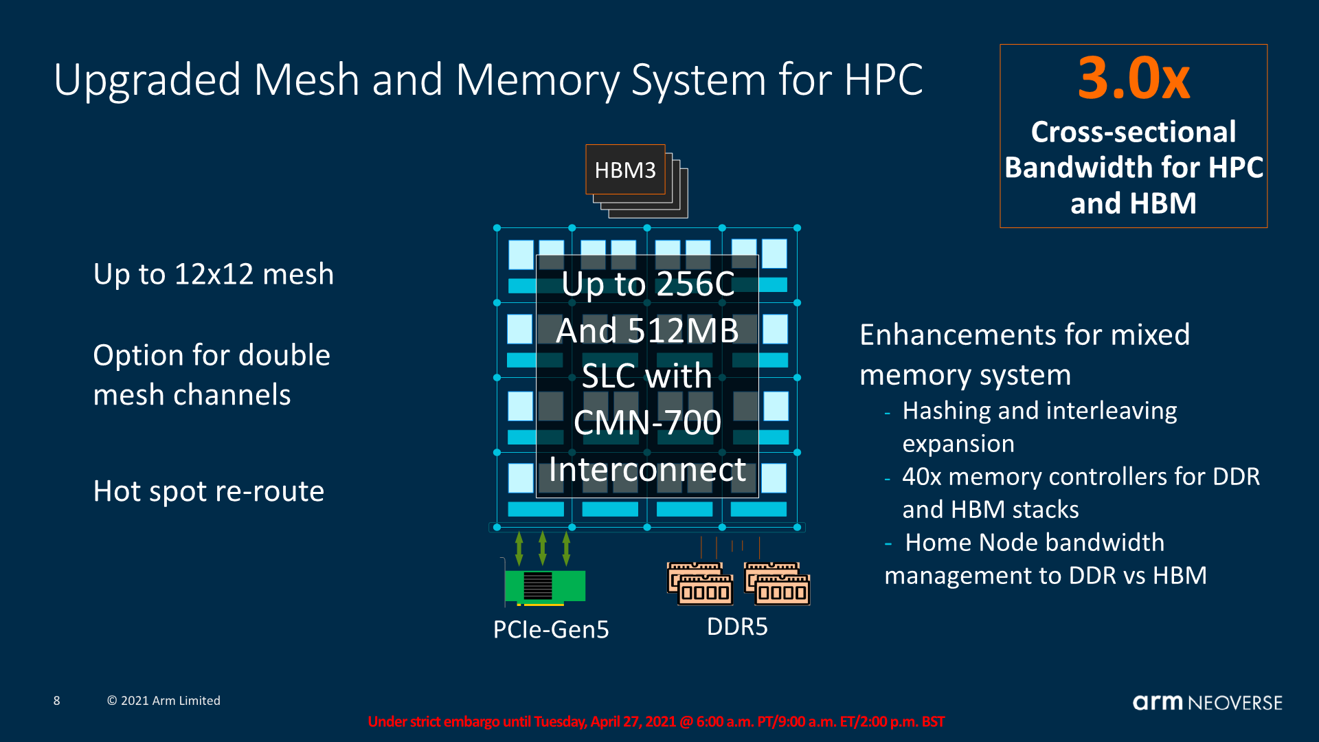
In terms of the memory capabilities, we noted that Arm expects hybrid architecture designs which would employ not only many more DDR memory controllers, but also integrate HBM memory. SiPearl’s Rhea chip is again such a confirmed design with 4x HBM2E stacks and 4-6 DDR5 memory controllers. The CMN-700 would be able to deal with such memory arrangements and properly manage the bandwidth and traffic across the heterogenous memory architectures.
Arm quotes a 3x increase in cross-sectional bandwidth in the mesh. Part of this is achieved through generational higher mesh frequencies, but the new design also most importantly now allows for doubled mesh channels between nodes. A mesh channel is still 256b wide with dedicated read and write ports, so a doubled-up design is essentially 2x256b in each direction. Arm discloses mesh frequencies of around 2GHz, so a 12x12 mesh with doubled up channels, if my math isn’t wrong, would result in cross-sectional bandwidth of around 3TB/s.
We asked Arm if the new mesh would be capable of more exotic 3D routing in terms of the direct interconnections between the nodes, but alas for this generation it’s still “only” limited to a 2D layout.
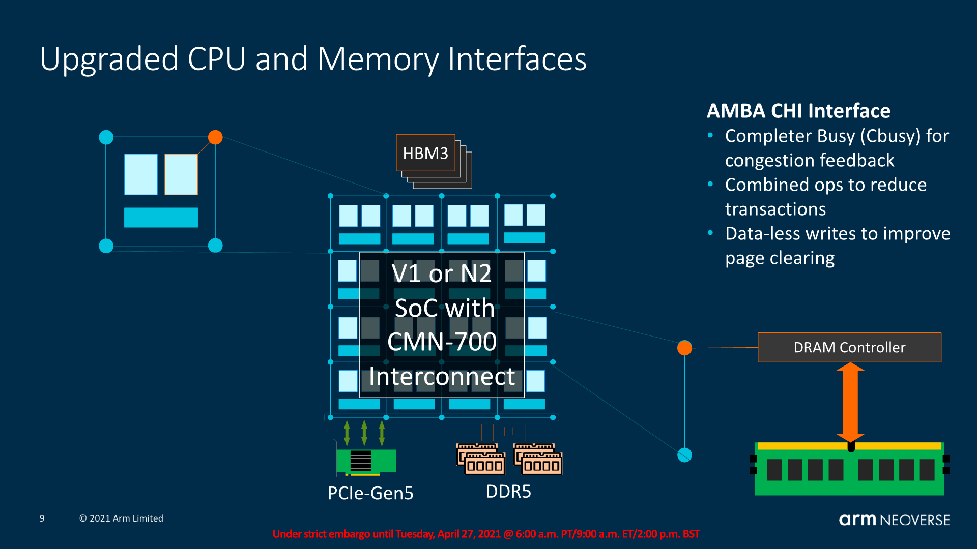
As noted in the V1 system features, CBusy is a new CPU-Mesh feature to alleviate mesh traffic congestions under high load, varying the CPU’s traffic requirements. There’s also general traffic improvements such as combining operations to reduce operations, or straightforward operations such as data-less writes to pages (Writing a page to all 0’s can be done with only one transaction, instead of writing zero to each cache line).
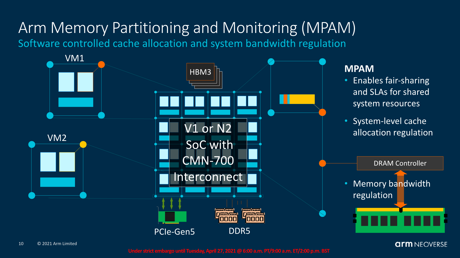
MPAM, again as explained in the earlier CPU section, helps traffic managing across independent workloads on a system such as VMs, ensuring QoS for SLA requirements, and general resource allocations across the entities in the system.
The CMN-600 this generation already had support for CCIX 1.1, which had been employed in designs such as the Altra Q. The CMN-700 now also introduces CCIX 2.0, as well as CXL compatibility.
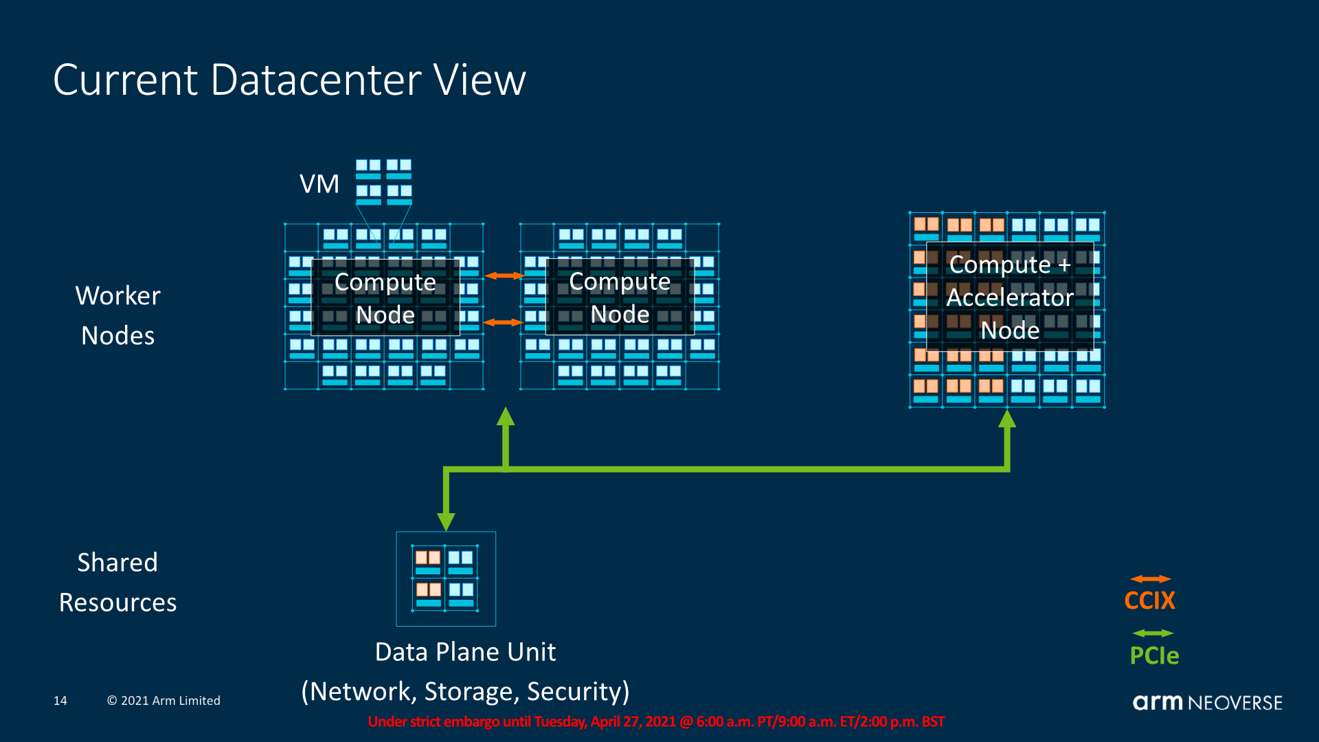
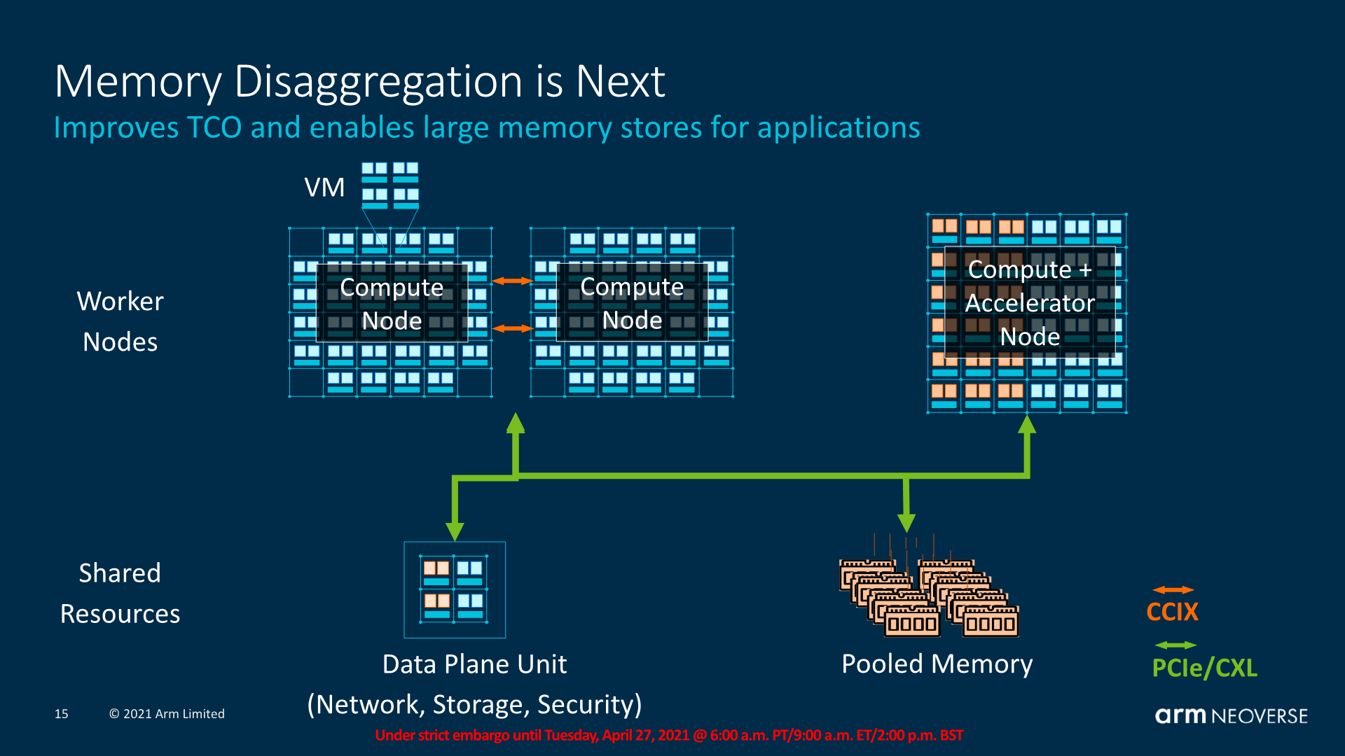
Besides operating with coherent accelerators over PCIe, Arm also sees memory disaggregation being a thing in the future, where we would see large pools of memory addressable by both the CPU clusters as well as the compute or accelerator nodes in a coherent fashion.
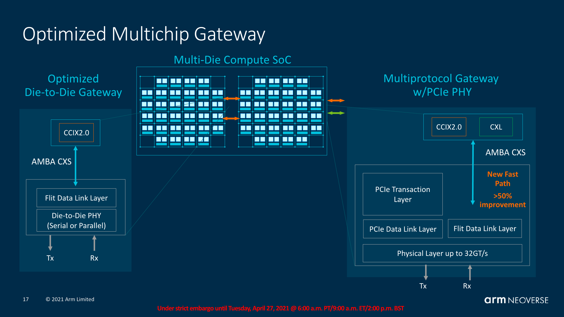
CCIX 2.0 is important for future multi-die and multi-socket designs as it’s allowed to get rid of the PCIe transaction and physical layers for a more closed generic link layer and PHY. One big disadvantage of the previous generation implementation, for example in multi-socket systems, was that it had tremendous latency penalties to cross all these different layers and protocols. We’ve seen the effect of this in our core-to-core test in the review of the Ampere Altra where the chip fared terribly in this regard.
The new CMN-700 and CCIX 2.0 connectivity promises to solve those very high latencies as well as the behaviour of requesting a remote socket cache line when talking between two cores in a local socket. This is not only important for socket-to-socket communications but also directly applies to chiplet-to-chiplet designs. It’s to be noted that Arm designs here still have to translate between AMBA CHI and CCIX 2.0 for such traffic, and whilst it’s much improved to what we’ve seen in the CCIX 1.1 implementations, it’s likely still not to be quite as performant as fully native protocol handling as for example Intel and AMD solutions.
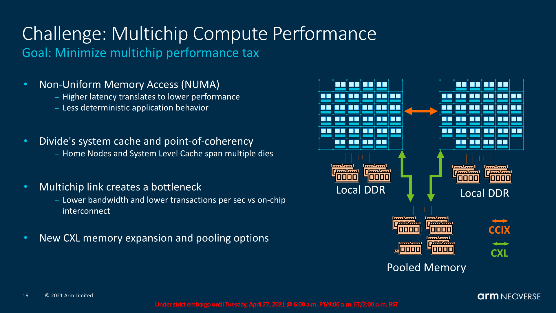
In multi-chip systems where there’s a disaggregation of memory through NUMA domains can result in performance hits when working on the same data. An alleviation of such scenarios is the division of the home node coherency across two chips (This is why the CMN-700 is advertised as up to 512 cores in a “system”). This has disadvantages as the multi-chip link can create a bottleneck, but then it’s also possible to architect exotic designs such as having pooled memory with equal access between two chips.
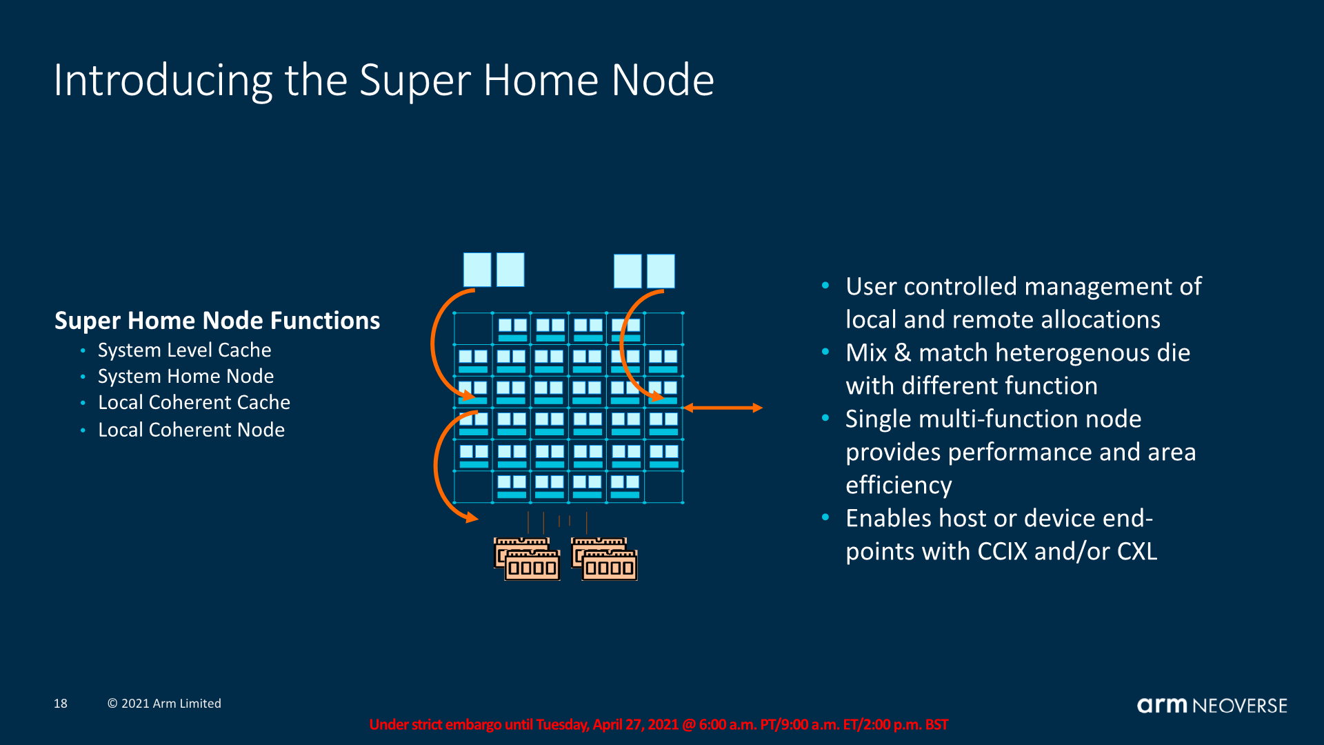
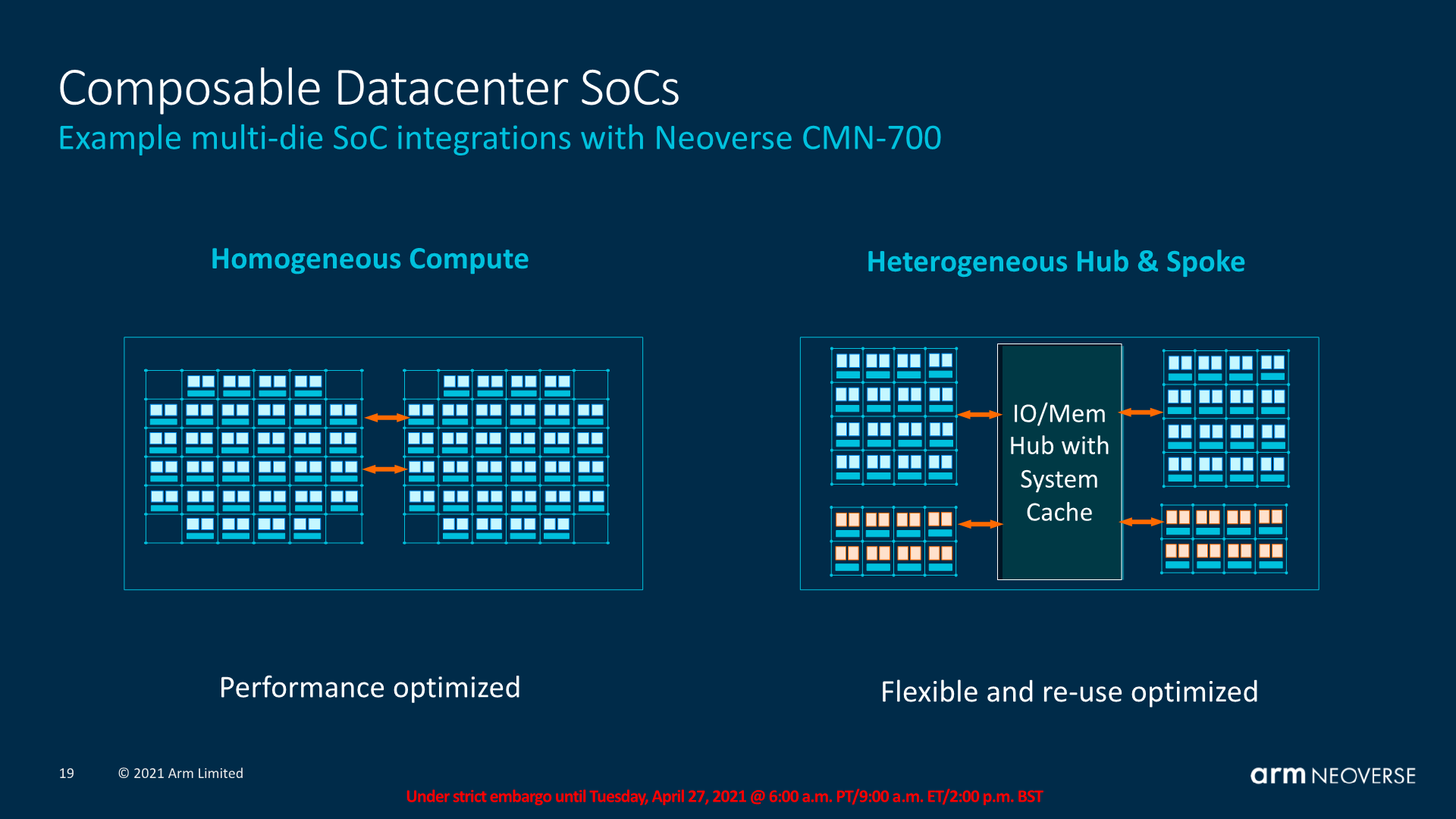
By now most readers will be familiar with AMD’s chiplet approach, and it’s a general architecture most vendors are heading towards given the slow-down of Moore’s law. Arm’s CMN-700 also allows for designs that are eerily similar to what AMD uses today, where a system can have a central IO Hub along with auxiliary compute dies.
We can have more traditional chip designs simply interconnected to each other, or more exotic designs with possible heterogenous chiplet architectures.
In the latter, Arm introduces the notion of a “Super Home Node” which acts as the central coherency point. In essence, this is simply just another mesh, but in theory it could be operated with no cores and simply just house an SLC (or none), and the central snoop filter handling coherency across all cores. In such an architecture, the SLC within that die would act as an L4 while the SLC in the mesh of a chiplet would act as an L3. There’s a bit of a mish-mash in terms of terminology here as we’re adding layers and chiplets, but I hope most will understand the hierarchy.


95 Comments
View All Comments
mode_13h - Wednesday, April 28, 2021 - link
Ah, yes! wikichip says of Zen 1:> Accordingly the peak throughput is four SSE/AVX-128 instructions
> or two AVX-256 instructions per cycle.
And Zen 2:
> This improvement doubles the peak throughput of AVX-256 instructions to four per cycle
Wow!
mode_13h - Tuesday, April 27, 2021 - link
What's SLC? I figured it was Second-Level Cache, until I saw the slide referencing "SLC -> L2 traffic"."System Level Cache", maybe? Could it be the term they use instead of L3 or LLC?
Thala - Tuesday, April 27, 2021 - link
I think you are totally right - SLC == LLC.Thala - Tuesday, April 27, 2021 - link
Quick addition. The term SLC is more popular lately, as it emphasize that the cache is not only shared among the cores but also with the system (GPU, DMAs etc).mode_13h - Wednesday, April 28, 2021 - link
Thanks. I guess I should've just waited until I'd finished reading it, because the interconnect slide made it abundantly clear.Now, I'm wondering about this "snoop filter" and why so much RAM is needed for it, when Graviton 2 & Altra have so little SLC. So, I gather it's not like tag RAM, then? Does it index the L2 of the adjacent cores, or something like that?
mode_13h - Tuesday, April 27, 2021 - link
Question and corrections on Page 6: PPA & ISO Performance ProjectionsWhat do the colors on the chip plots mean?
> Only losing out 10% IPC versus the N1
I'm sure that's meant to say "V1".
> In terms of absolute IPC improvements
Huh? These are definitely "relative IPC improvements" or just "IPC improvements".
Calin - Wednesday, April 28, 2021 - link
AWS share by vendor type: It should have been "Vendor A" and "Vendor I"mode_13h - Wednesday, April 28, 2021 - link
That slide was provided by ARM and I think they're trying to have at least the *appearance* of maintaining anonymity, even if the identities are abundantly clear.Also, you realize that their Vendor A is your Vendor I, right?
serendip - Wednesday, April 28, 2021 - link
How does the narrower front end and shallower pipeline of the N2 compare to Apple's M1? I'm thinking about how this could translate to the A78 successor, if that uses an evolution of the X1 core with improvements from N2 brought in.mode_13h - Thursday, April 29, 2021 - link
Good point. It suggests the A78+1 will perform < N2.Although, a derivative X-core would likely be > N2.