The Ampere Altra Review: 2x 80 Cores Arm Server Performance Monster
by Andrei Frumusanu on December 18, 2020 6:00 AM EST- Posted in
- Servers
- Neoverse N1
- Ampere
- Altra
Compiling LLVM, NAMD Performance
As we’re trying to rebuild our server test suite piece by piece – and there’s still a lot of work go ahead to get a good representative “real world” set of workloads, one more highly desired benchmark amongst readers was a more realistic compilation suite. Chrome and LLVM codebases being the most requested, I landed on LLVM as it’s fairly easy to set up and straightforward.
git clone https://github.com/llvm/llvm-project.gitcd llvm-projectgit checkout release/11.xmkdir ./buildcd ..mkdir llvm-project-tmpfssudo mount -t tmpfs -o size=10G,mode=1777 tmpfs ./llvm-project-tmpfscp -r llvm-project/* llvm-project-tmpfscd ./llvm-project-tmpfs/buildcmake -G Ninja \ -DLLVM_ENABLE_PROJECTS="clang;libcxx;libcxxabi;lldb;compiler-rt;lld" \ -DCMAKE_BUILD_TYPE=Release ../llvmtime cmake --build .We’re using the LLVM 11.0.0 release as the build target version, and we’re compiling Clang, libc++abi, LLDB, Compiler-RT and LLD using GCC 10.2 (self-compiled). To avoid any concerns about I/O we’re building things on a ramdisk – on a 4KB page system 5GB should be sufficient but on the Altra’s 64KB system it used up to 9.5GB, including the source directory. We’re measuring the actual build time and don’t include the configuration phase as usually in the real world that doesn’t happen repeatedly.
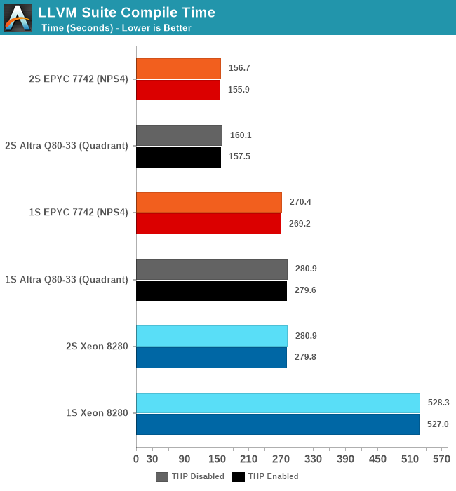
The Altra Q80-33 here performs admirably and pretty much matches the AMD EPYC 7742 both in 1S and 2S configurations. There isn’t exact perfect scaling between sockets because this being a actual build process, it also includes linking phases which are mostly single-threaded performance bound.
Generally, it’s interesting to see that the Altra here fares better than in the SPEC 502.gcc_r MT test – pointing out that real codebases might not be quite as demanding as the 502 reference source files, including a more diverse number of smaller files and objects that are being compiled concurrently.
NAMD
Another rather popular benchmark tool that we’ve actually seen being used by vendors such as AMD in their marketing materials when showcasing HPC performance for their server chips is NAMD. This actually quite an interesting adventure in terms of compiling the tool for AArch64 as essentially there little to no proper support for it. I’ve used the latest source drop, essentially the 2.15alpha / 3.0alpha tree, and compiled it from scratch on GCC 10.2 using the platform’s respective -march and -mtune targets.
For the Xeon 8280 – I did not use the AVX512 back-end for practical reasons: The code which introduces an AVX512 algorithm and was contributed by Intel engineers to NAMD has no portability to compilers other than ICC. Beyond this being a code-path that has no relation with the “normal” CPU algorithm – the reliance on ICC is something that definitely made me raise my eyebrows. It’s a whole other discussion topic on having a benchmark with real-world performance and the balance of having an actual fair and balanced apple to apples comparison. It’s something to revisit in the future as I invest more time into looking the code and see if I can port it to GCC or LLVM.
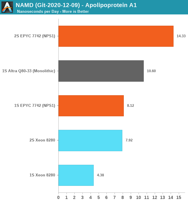
For the single-socket numbers – we’re using the multicore variant of the tool which has predictable scaling across a single NUMA node. Here, the Ampere Altra Q80-33 performed amazingly well and managed to outperform the AMD EPYC 7742 by 30% - signifying this is mostly a compute-bound workload that scales well with actual cores.
For the 2S figures, using the multicore binaries results in undeterministic performance – the Altra here regressed to 2ns/day and the EPYC system also crashed down to 4ns/day – oddly enough the Xeon system had absolutely no issue in running this properly as it had excellent performance scaling and actually outperforms the MPI version. The 2S EPYC scales well with the MPI version of the benchmark, as expected.
Unfortunately, I wasn’t able to compile an MPI version of NAMD for AArch64 as the codebase kept running into issues and it had no properly maintained build target for this. In general, I felt like I was amongst the first people to ever attempt this, even though there are some resources to attempt to help out on this.
I also tried running Blender on the Altra system but that ended up with so many headaches I had to abandon the idea – on CentOS there were only some really old build packages available in the repository. Building Blender from source on AArch64 with all of its dependencies ends up in a plethora of software packages which simply assume you’re running on x86 and rely on basic SSE intrinsics – easy enough to fix that in the makefiles, but then I hit some other compilation errors after which I lost my patience. Fedora Linux seemed to be the only distribution offering an up-to-date build package for Blender – but I stopped short of reinstalling the OS just to benchmark Blender.
So, while AArch64 has made great strides in the past few years – and the software situation might be quite good for server workloads, it’s not all rosy and we’re still have ways to go before it can be considered a first-class citizen in the software ecosystem. Hopefully Apple’s introduction of Apple Silicon Macs will accelerate the Arm software ecosystem.


148 Comments
View All Comments
Wilco1 - Friday, December 18, 2020 - link
How exactly is it big? It's tiny for a server chip - 80 cores at about half the die size of a typical 28-core Xeon (~700mm^2). And TSMC 7nm yield is extremely good even for much larger chips like GPUs.Ithaqua - Friday, December 18, 2020 - link
Plus as with all chips, there may be a 64 / 48 / 32 core version which are just standard chips with the defective core block turned off.eastcoast_pete - Saturday, December 19, 2020 - link
Note I wrote "quite big", and by transistor count, it's a larger CPU, expected for a server chip. As for the Xeon, how high is Intel's yield for the 28 core Xeon, and that after how many years on 14 nm+++ (etc)? So, if you have a yield number for this 80 core Ampere chip, please share it.Wilco1 - Saturday, December 19, 2020 - link
It's larger than a mobile SoC, but small for a server chip thanks to Arm's tiny cores and the high density of TSMC 7nm. See https://www.anandtech.com/show/16028/better-yield-... for the defect rate, and from that a simple yield calculator gives 71% for a 350mm^2 die. That's before you fix SRAM defects or harvest dies for the lower-end SKUs. So we conclude yield is very good.eastcoast_pete - Saturday, December 19, 2020 - link
Glad to read that you've proven Andrei wrong, so maybe you should write these reviews. Here a direct quote from the first page of the review (also, take a look at the pictures: "The chip itself is absolutely humongous and amongst the current publicly available processors is the biggest in the industry, out-sizing AMD’s SP3 form-factor packaging, coming in at around 77 x 66.8mm – about the same length but considerably wider than AMD’s counterparts."Wilco1 - Saturday, December 19, 2020 - link
How ignorant can you be? Obviously the chip and silicon die have different sizes. The chip is large because it has many pins. The silicon die is a tiny fraction of the chip. We're discussing the size of the silicon die here, not the size of the chip. Completely different things.mode_13h - Sunday, December 20, 2020 - link
It'd be less confusing if you'd talk about the "package" dimensions.I think die and chip are traditionally synonymous. For instance, a package with multiple dies is traditionally called a MCM (Multi-Chip Module).
Wilco1 - Monday, December 21, 2020 - link
Look at Andrei's quote above, there isn't a well-defined term - people use chip/CPU/package etc as synonyms.mode_13h - Monday, December 21, 2020 - link
But it's not hard to see how "chip" can cause confusion. So, why not avoid it entirely, and just say either "die" or "package".Only a troll or someone with an agenda could be against clear communication.
Wilco1 - Monday, December 21, 2020 - link
It's hard to imagine how anyone sane can believe that a "chip measuring 77 x 66.8mm" (6 times the reticle limit!) is referring to the die size rather than the package. Andrei's quote even uses the word package. So maybe you're right and eastcoast_pete was just trolling.