Qualcomm Details The Snapdragon 888: 3rd Gen 5G & Cortex-X1 on 5nm
by Andrei Frumusanu on December 2, 2020 10:00 AM EST- Posted in
- Mobile
- Qualcomm
- Smartphones
- SoCs
- 5G
- Cortex A78
- Cortex X1
- Snapdragon 888
Triple ISPs: Concurrent Triple-Camera Usage
Interestingly enough, during yesterday’s keynote event, Qualcomm described themselves as a camera company, which is a funny way to see things, but actually somewhat makes sense given the large leaps in smartphone camera capture capabilities over the recent years.
The new Snapdragon 888 pushes the envelope in terms camera abilities by adding a whole new independent third ISP to the SoC, allowing the SoC to now run three independent camera modules concurrently, opening up new use cases for vendors and camera applications.

The new triple-ISP architecture now increases the overall pixel processing throughput by 35% to 2.7Gigapixels/s, allowing for concurrent usage of up to three 28MP sensors with zero shutter lag captures. Alternatively, you can use a combination of 64+25MP sensors with ZSL, or a single 84MP sensor with ZSL. There’s still also support for ultra-high-resolution sensors up to 200MP, but image captures here don’t support ZSL.
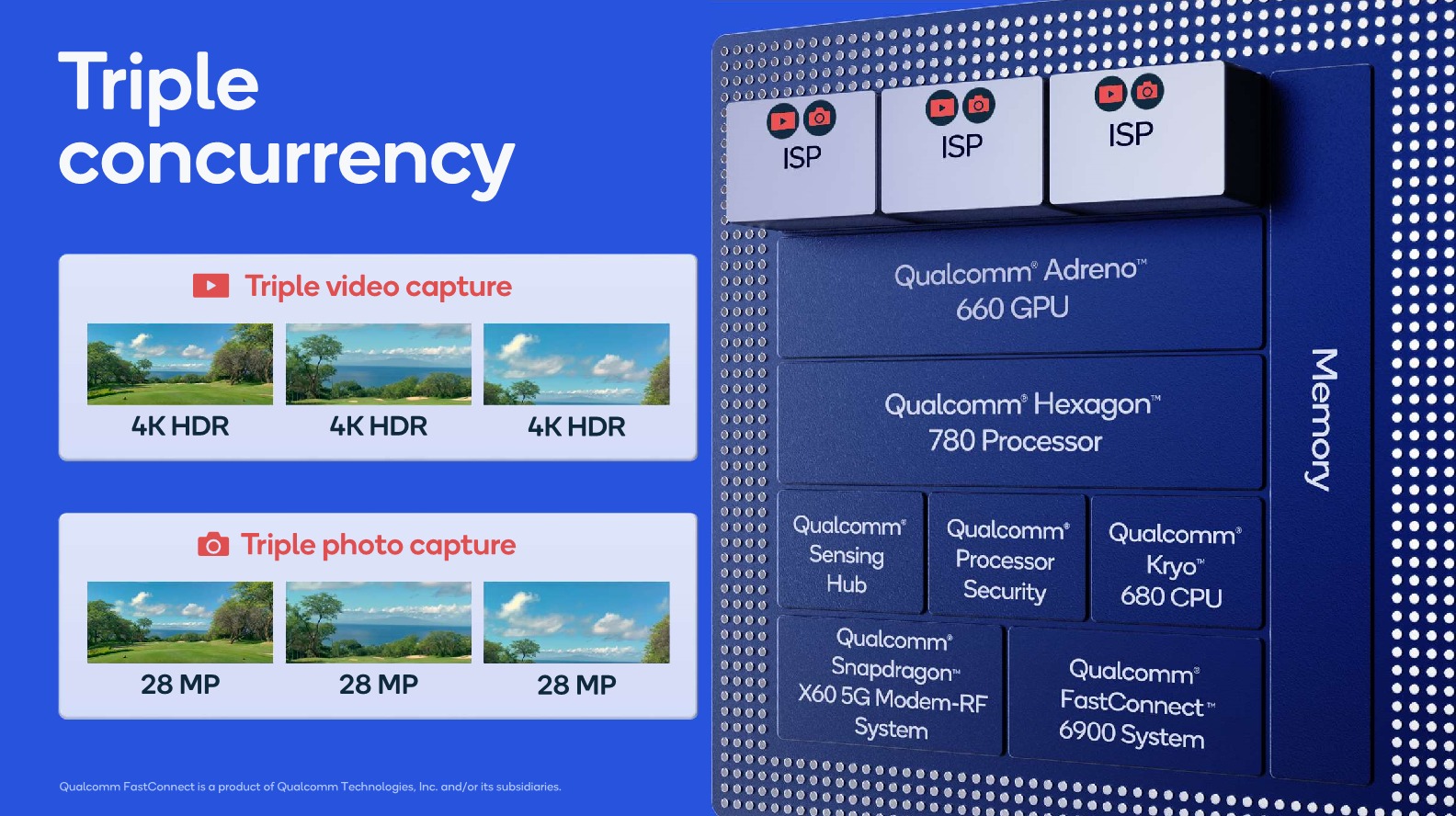
Allowing concurrent captures of three sensors now allows for the holy trifecta of ultra-wide-angle, wide-angle and telephoto modules to capture a scene at the same time, allowing for more interesting use-cases such as image stitching and image fusion to happen to seamlessly.
One interesting capability that Qualcomm was advertising is triple-stream 4K HDR video recording. That’s a bit of an odd-ball use-case as I do wonder about the practical benefits, but I do at least hope that the new triple ISP system allows for more seamless switching and zooming in and out between the various camera modules during video recording.
Video recording capabilities this year don’t seem to have changed, compared to the Snapdragon 865. This means 4K120 or 8K30 are still the peak capture modes, supporting also slow-motion of 720p960. Formats are also unchanged, with HEVC encoding in HDR formats such as HDR10+ or Dolby Vision being supported.
AV1 decoding didn’t make the cut this year unfortunately, which means wide-spread adoption in mobile for the codec will be delayed for another year.
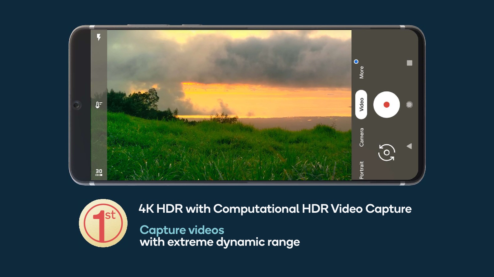
While the video encoding formats haven’t changed, the image processing capabilities for HDR capture has. Thanks to the new ISPs and the raw performance throughput, the new Snapdragon 888 will be able to capture 4K HDR footage with the more advanced computational HDR processing being applied on each and every frame of the video.

Qualcomm claims that the new ISP in the Snapdragon 888 is the first to support new next-generation staggered HDR sensors.
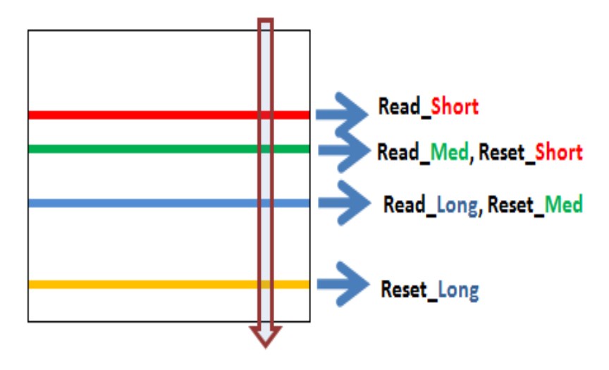
Source: OmniVision
These are sensors that can have multiple rolling shutters, meaning sensor line readouts, active at the same time on the sensor. Instead of taking multiple exposures one at a time sequentially by scanning out the sensor matrix from start to finish, the sensor will start another exposure immediately after the completed line read-out, reducing the time in-between exposures greatly. This should allow for significant less motion ghosting between the exposures and a sharper resulting recombined HDR image capture than current generation sensors which only have a single active line readout on the sensor.
While we haven’t actually heard of such sensors from Samsung or Sony yet, Qualcomm is adamant that we’ll be seeing smartphones in 2021 employing this new technology.

A further improvement for still-picture captures is the advancement of the new multi-frame noise reduction engines inside of the ISPs. It’s said that the quality of the noise reduction has been improved this generation, allowing for even better low-light captures with the native capture mode (no computational photography).


123 Comments
View All Comments
name99 - Wednesday, December 2, 2020 - link
From the outside, the problem appears to be that ARM is too deferential to its customers (one of the things that nV could fix if they get control...)In particular (compare with Apple) ARM appears unwilling to just do something new and aggressive and hope that it will be picked up when it's ready.
This might seem reasonable, but the problem is that your main customers are companies like Samsung and Qualcomm, the gang that couldn't shoot straight. Both (still!) seem utterly unaware that Moore's law is still a thing, and that the needs of devices evolve with time. So they both insist their priorities are smallest cheapest cores possible -- until there's a mad scramble to match whatever Apple is doing.
This foolishness has been most obvious with the A55. Sure, maybe in some technical sense the A55 is good enough wrt performance and energy and did not need to be updated for those reasons. BUT refusing to update it locks the ISA at v8.2.
(Does anyone know how this is handled given that in theory the A78 supports some v8.3 instructions? Is the rule just that you don't use those instructions on a dynamiq A78+A55 system?)
So QC and SS are stuck. Because n years ago they were too stupid to see the big picture, that future small cores would need to track the evolving ARM ISA, they've held back what their large cores can do. A more dynamic ARM should probably just have ignored whatever they said and switched to a model like Apple that updates the large and small cores in lockstep every year.
GeoffreyA - Thursday, December 3, 2020 - link
The magic is simple: Icestorm is quite likely an out-of-order design, which picks up the performance quite a bit. And as for the extra power that comes along with out of order, they probably got it right down with enough optimisation/clever design (physical register files, micro-op cache, etc). Reminds me a bit of the comparison between Atom and Bobcat/Jaguar. For my part, I feel that in-order designs aren't really worth the supposed power savings (except in some cases), so I don't know why these companies waste their time.GeoffreyA - Thursday, December 3, 2020 - link
Replying to brucethemoose.eastcoast_pete - Friday, December 4, 2020 - link
Does anyone here know for sure whether Apple's efficiency cores are indeed out-of-order designs? That might actually help explain the better performance and performance/Wh of their Ice Storm cores; and raise the question: why hasn't ARM updated its little core design? I guess one answer is because they didn't have to (yet).Lolimaster - Thursday, December 10, 2020 - link
Considering A77 is more efficient and powerful at the same frequency than the A55 which is really old. Increase it a bit in size with big update and extra budget and you the Apple "lpA76" cores.tuxRoller - Thursday, December 3, 2020 - link
The answer is... the old big cores are replaced by the new X series and become the new little (or mid) core.yeeeeman - Wednesday, December 2, 2020 - link
can't wait for battery life tests, although i suspect they will be a bit worse than tsmc 7nm.iphonebestgamephone - Thursday, December 3, 2020 - link
Why did they bother with 5nm then? Is this 5nm even cheaper than tsmc 7?SyukriLajin - Thursday, December 3, 2020 - link
because apple have been marketing 5nm, and they can't sell "the best [android] soc in the market" with 7nm, especially when their android competitors are also moving to 5nm. the efficiency difference might be small, but marketing impact is big enough to ignore. plus most phones running this chip in 2021 probably have 4000mAh+ batteries in it anyway, wouldn't make any impact in consumer products.iphonebestgamephone - Thursday, December 10, 2020 - link
Do the general public care more about nm or antutu? Or is it that oems would be more likely to get the 5nm one?