Qualcomm Details The Snapdragon 888: 3rd Gen 5G & Cortex-X1 on 5nm
by Andrei Frumusanu on December 2, 2020 10:00 AM EST- Posted in
- Mobile
- Qualcomm
- Smartphones
- SoCs
- 5G
- Cortex A78
- Cortex X1
- Snapdragon 888
Triple ISPs: Concurrent Triple-Camera Usage
Interestingly enough, during yesterday’s keynote event, Qualcomm described themselves as a camera company, which is a funny way to see things, but actually somewhat makes sense given the large leaps in smartphone camera capture capabilities over the recent years.
The new Snapdragon 888 pushes the envelope in terms camera abilities by adding a whole new independent third ISP to the SoC, allowing the SoC to now run three independent camera modules concurrently, opening up new use cases for vendors and camera applications.

The new triple-ISP architecture now increases the overall pixel processing throughput by 35% to 2.7Gigapixels/s, allowing for concurrent usage of up to three 28MP sensors with zero shutter lag captures. Alternatively, you can use a combination of 64+25MP sensors with ZSL, or a single 84MP sensor with ZSL. There’s still also support for ultra-high-resolution sensors up to 200MP, but image captures here don’t support ZSL.
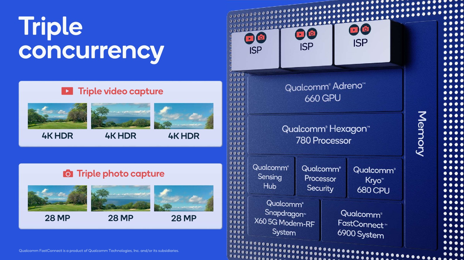
Allowing concurrent captures of three sensors now allows for the holy trifecta of ultra-wide-angle, wide-angle and telephoto modules to capture a scene at the same time, allowing for more interesting use-cases such as image stitching and image fusion to happen to seamlessly.
One interesting capability that Qualcomm was advertising is triple-stream 4K HDR video recording. That’s a bit of an odd-ball use-case as I do wonder about the practical benefits, but I do at least hope that the new triple ISP system allows for more seamless switching and zooming in and out between the various camera modules during video recording.
Video recording capabilities this year don’t seem to have changed, compared to the Snapdragon 865. This means 4K120 or 8K30 are still the peak capture modes, supporting also slow-motion of 720p960. Formats are also unchanged, with HEVC encoding in HDR formats such as HDR10+ or Dolby Vision being supported.
AV1 decoding didn’t make the cut this year unfortunately, which means wide-spread adoption in mobile for the codec will be delayed for another year.
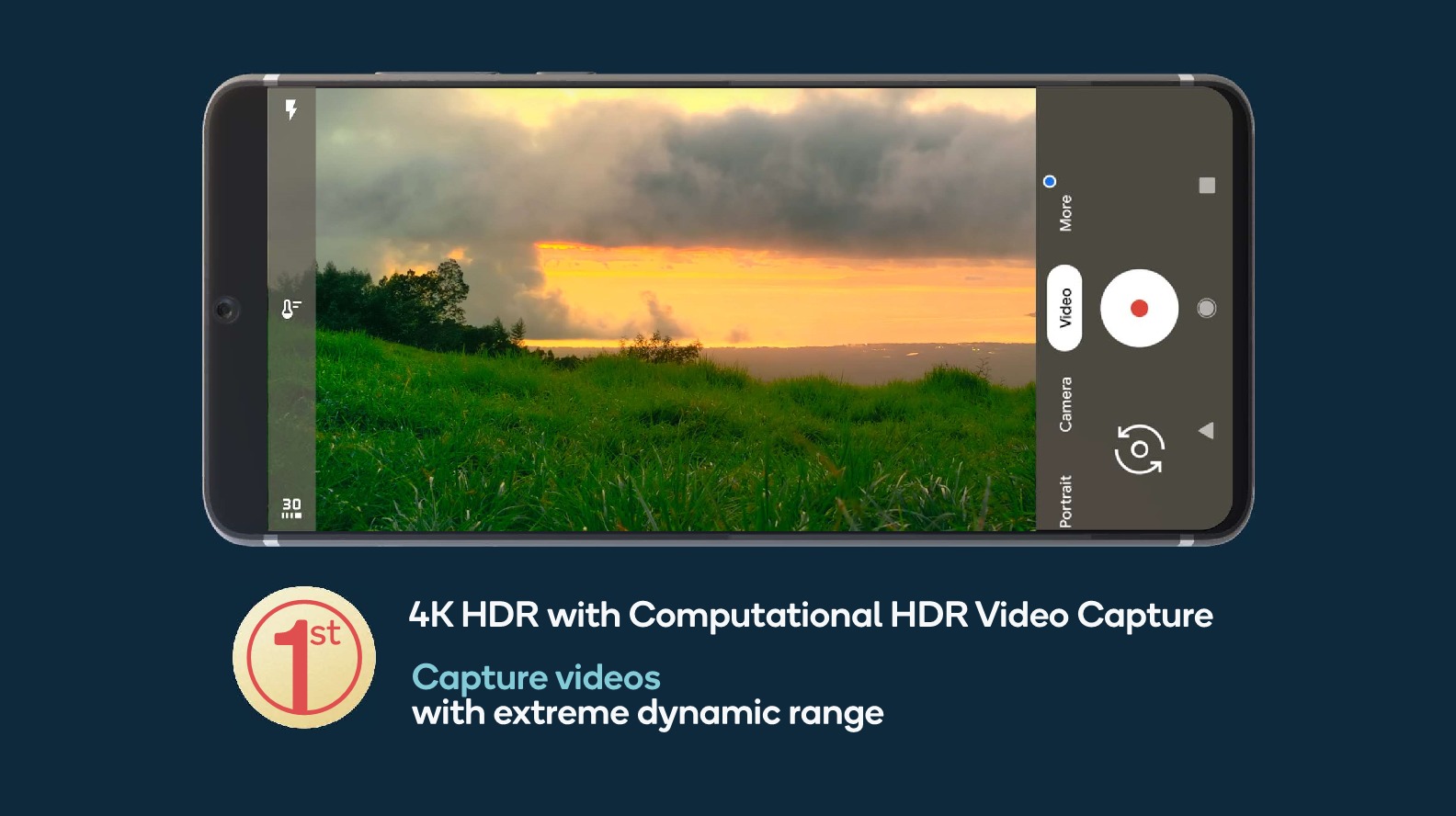
While the video encoding formats haven’t changed, the image processing capabilities for HDR capture has. Thanks to the new ISPs and the raw performance throughput, the new Snapdragon 888 will be able to capture 4K HDR footage with the more advanced computational HDR processing being applied on each and every frame of the video.
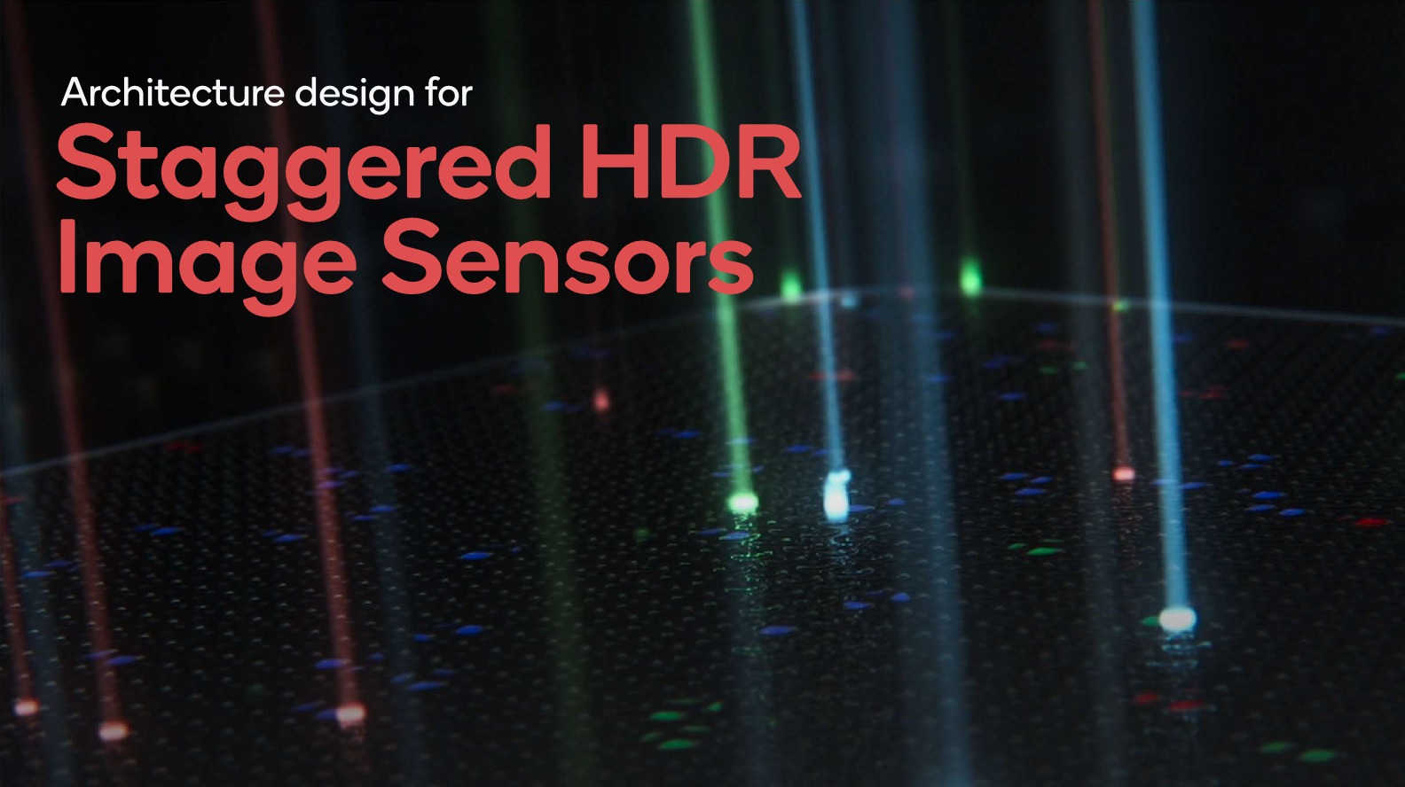
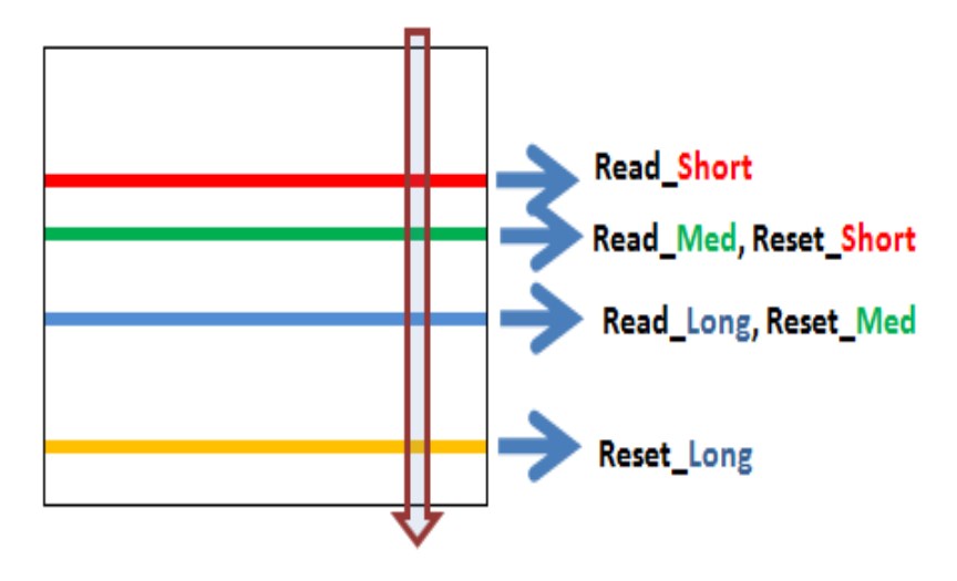
Qualcomm claims that the new ISP in the Snapdragon 888 is the first to support new next-generation staggered HDR sensors.
Source: OmniVision
These are sensors that can have multiple rolling shutters, meaning sensor line readouts, active at the same time on the sensor. Instead of taking multiple exposures one at a time sequentially by scanning out the sensor matrix from start to finish, the sensor will start another exposure immediately after the completed line read-out, reducing the time in-between exposures greatly. This should allow for significant less motion ghosting between the exposures and a sharper resulting recombined HDR image capture than current generation sensors which only have a single active line readout on the sensor.
While we haven’t actually heard of such sensors from Samsung or Sony yet, Qualcomm is adamant that we’ll be seeing smartphones in 2021 employing this new technology.

A further improvement for still-picture captures is the advancement of the new multi-frame noise reduction engines inside of the ISPs. It’s said that the quality of the noise reduction has been improved this generation, allowing for even better low-light captures with the native capture mode (no computational photography).


123 Comments
View All Comments
iphonebestgamephone - Sunday, December 6, 2020 - link
Mediatek gonna trash qualcomm this year!!ChrisGX - Sunday, December 13, 2020 - link
7FFP has the same density as 7FF but has a number of improvements. The dense TSMC process is 7FF+ (also known as N7+) and it is an EUV node. The dense node you refer to is 7FF+. Somebody seems to have wrongly assumed that P refers to plus - it doesn't. Still, the error after exchange by many hands has become pervasive on the web.EMMVIN - Thursday, December 3, 2020 - link
When can we expect the detailed analysis of the soc and benchmark comparisons. There is nothing out there that is as detailed as yours. Hope you guys already have an early sample to test :)tuxRoller - Friday, December 4, 2020 - link
I'm curious if the move to samsung negatively affected clocking. If not, then this is a really cheap move in favor of their later 888+.vladx - Friday, December 4, 2020 - link
Still no AV1 decoding at least? Pathetic from QualcommJames5mith - Saturday, December 5, 2020 - link
"allowing for the vastly increased workload handoff time between the different execution engines"So it's much slower now?
peevee - Thursday, December 10, 2020 - link
"multi-frame noise reduction engines inside of the ISPs. It’s said that the quality of the noise reduction has been improved this generation, allowing for even better low-light captures with the native capture mode (no computational photography)"What you have described IS computational photography.
KarlKastor - Saturday, December 12, 2020 - link
@AndreiI can't really understand, where you see the 7LPP in a disadvantage in comparison to N7.
If you compare the 765G with the middle cores of the 855, you see similar power draw.
The comparison to the Kirin show higher frequency and higher power for the Kirin. I can't see a winner here. You can't look at the efficiency score. The performance is higher with the Kirin because of the bigger Caches. Double the L2 and 4x L3. Memory bandwidth and SL-Cache is bigger too.
ChrisGX - Sunday, December 13, 2020 - link
You have a point in connection to the N7 but you are on shakier ground with regard to the N7P and N7+. The Semiwiki article shows the density advantage of N7+ process (otherwise known as 7FF+ and mislabelled in the article as 7FFP) used on the Kirin 990 5G SoC. TSMC data likewise underscores the greater density and energy efficiency of the N7+ process.https://consumer.huawei.com/ae-en/community/detail...
https://semiwiki.com/semiconductor-manufacturers/s...
https://pr.tsmc.com/english/news/2010
Bunny13 - Wednesday, January 6, 2021 - link
The more I know about the 888, the more disappointed I am