Apple Announces The Apple Silicon M1: Ditching x86 - What to Expect, Based on A14
by Andrei Frumusanu on November 10, 2020 3:00 PM EST- Posted in
- Apple
- Apple A14
- Apple Silicon
- Apple M1
From Mobile to Mac: What to Expect?
To date, our performance comparisons for Apple’s chipsets have always been in the context of iPhone reviews, with the juxtaposition to x86 designs being a rather small footnote within the context of the articles. Today’s Apple Silicon launch event completely changes the narrative of what we portray in terms of performance, setting aside the typical apples vs oranges comparisons people usually argument with.
We currently do not have Apple Silicon devices and likely won’t get our hands on them for another few weeks, but we do have the A14, and expect the new Mac chips to be strongly based on the microarchitecture we’re seeing employed in the iPhone designs. Of course, we’re still comparing a phone chip versus a high-end laptop and even a high-end desktop chip, but given the performance numbers, that’s also exactly the point we’re trying to make here, setting the stage as the bare minimum of what Apple could achieve with their new Apple Silicon Mac chips.
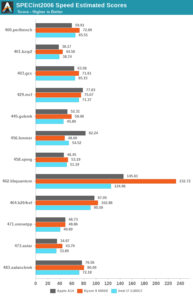
The performance numbers of the A14 on this chart is relatively mind-boggling. If I were to release this data with the label of the A14 hidden, one would guess that the data-points came from some other x86 SKU from either AMD or Intel. The fact that the A14 currently competes with the very best top-performance designs that the x86 vendors have on the market today is just an astonishing feat.
Looking into the detailed scores, what again amazes me is the fact that the A14 not only keeps up, but actually beats both these competitors in memory-latency sensitive workloads such as 429.mcf and 471.omnetpp, even though they either have the same memory (i7-1185G7 with LPDDR4X-4266), or desktop-grade memory (5950X with DDR-3200).
Again, disregard the 456.hmmer score advantage of the A14, that’s majorly due to compiler discrepancies, subtract 33% for a more apt comparison figure.
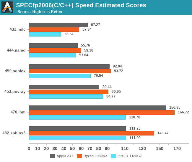
Even in SPECfp which is even more dominated by memory heavy workloads, the A14 not only keeps up, but generally beats the Intel CPU design more often than not. AMD also wouldn’t be looking good if not for the recently released Zen3 design.
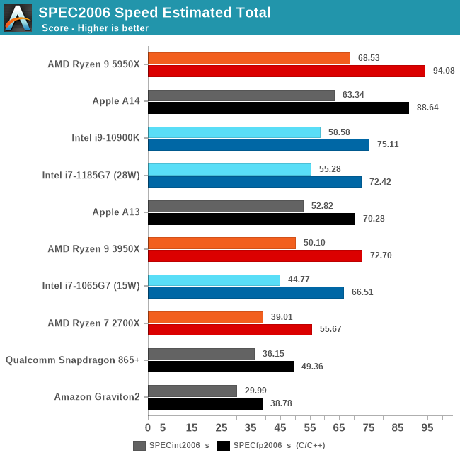
In the overall SPEC2006 chart, the A14 is performing absolutely fantastic, taking the lead in absolute performance only falling short of AMD’s recent Ryzen 5000 series.
The fact that Apple is able to achieve this in a total device power consumption of 5W including the SoC, DRAM, and regulators, versus +21W (1185G7) and 49W (5950X) package power figures, without DRAM or regulation, is absolutely mind-blowing.
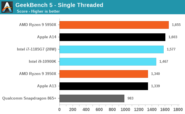
There’s been a lot of criticism about more common benchmark suites such as GeekBench, but frankly I've found these concerns or arguments to be quite unfounded. The only factual differences between workloads in SPEC and workloads in GB5 is that the latter has less outlier tests which are memory-heavy, meaning it’s more of a CPU benchmark whereas SPEC has more tendency towards CPU+DRAM.
The fact that Apple does well in both workloads is evidence that they have an extremely well-balanced microarchitecture, and that Apple Silicon will be able to scale up to “desktop workloads” in terms of performance without much issue.
Where the Performance Trajectory Finally Intersects
During the release of the A7, people were pretty dismissive of the fact that Apple had called their microarchitecture a desktop-class design. People were also very dismissive of us calling the A11 and A12 reaching near desktop level performance figures a few years back, and today marks an important moment in time for the industry as Apple’s A14 now clearly is able to showcase performance that’s beyond the best that Intel can offer. It’s been a performance trajectory that’s been steadily executing and progressing for years:
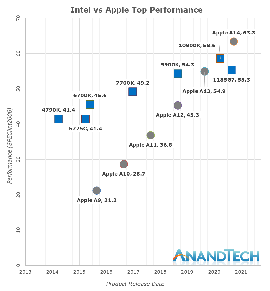
Whilst in the past 5 years Intel has managed to increase their best single-thread performance by about 28%, Apple has managed to improve their designs by 198%, or 2.98x (let’s call it 3x) the performance of the Apple A9 of late 2015.
Apple’s performance trajectory and unquestioned execution over these years is what has made Apple Silicon a reality today. Anybody looking at the absurdness of that graph will realise that there simply was no other choice but for Apple to ditch Intel and x86 in favour of their own in-house microarchitecture – staying par for the course would have meant stagnation and worse consumer products.
Today’s announcements only covered Apple’s laptop-class Apple Silicon, whilst we don’t know the details at time of writing as to what Apple will be presenting, Apple’s enormous power efficiency advantage means that the new chip will be able to offer either vastly increased battery life, and/or, vastly increased performance, compared to the current Intel MacBook line-up.
Apple has claimed that they will completely transition their whole consumer line-up to Apple Silicon within two years, which is an indicator that we’ll be seeing a high-TDP many-core design to power a future Mac Pro. If the company is able to continue on their current performance trajectory, it will look extremely impressive.


644 Comments
View All Comments
pcordes - Thursday, November 19, 2020 - link
Thanks for the microarchitectural testing and details!However, some current Intel / AMD numbers you use for comparison aren't right. (Also, your ROB-size and load/store buffers graphs are missing labels on the vertical axis; I assume that's time or cycles or something with.)
Intel since Skylake has 5-wide legacy decode (up from 4-wide in Haswell) and 6-wide fetch from the decoded-uop cache. (The issue/rename stage is still only 4-wide in Skylake, but widened to 5 in Ice Lake. Being wider earlier in the front-end can catch up after stalls, letting buffers between stages hide bubbles) https://en.wikichip.org/wiki/intel/microarchitectu...
https://en.wikichip.org/wiki/intel/microarchitectu...
(The decoders can also macro-fuse a cmp/jcc branch into 1 uop, so max decode throughput is actually 7 x86 instructions per clock, into 5 uops.)
AMD Zen 2 can decode up to 4 x86 instructions per clock. (Not sure if that includes fusion of cmp/jcc or not). This is probably where you got your 4-wide number that you claimed applied to Intel. But that's just legacy-decode. Most code spends a lot of time in non-huge loops, and they can run from the uop cache. Zen 2's decoded-uop cache can produce up to 8 uops/clock.
https://en.wikichip.org/wiki/amd/microarchitecture...
The actual bottleneck for sending instructions into the out-of-order back-end is the issue/rename stage as usual: 6 uops, but I think those can only come from up to 5 x86 instructions. I thought I remembered reading that Zen 1 could only sustain 6 uops / clock when running code that included some AVX 256-bit instructions or other 2-uop instructions. Maybe that changed with Zen2 (where most 256-bit SIMD instructions are still 1 uop), I don't have an AMD system to test on, and stuff like https://uops.info/ only tests throughput of single instructions, not a mix of integer, FP, and/or loads/store.
Anyway, Zen's front-end is at least 5-wide, and 6-wide for at least some purposes.
---
You seem to be saying M1 can do 4 FADDs *and* 4 FMULs in the same cycle. That doesn't make any sense with "only" 4 FP execution units. Perhaps you mean 4 FMAs per cycle? Or can each execution unit really accept 2 instructions in the same clock cycle, like Pentium 4's double-pumped integer ALUs?
That's only twice the throughput of Haswell/Skylake, or the same throughput if you take vector width into account, assuming Apple M1 doesn't have ARM SVE for wider vectors.
(Skylake has FMA units on ports 0 and 1, each 256-bit wide. FP mul / add also run on those same units, all with 4-cycle latency. So using FMAs instead of `vaddps` or `vmulps` gives Skylake twice the FLOPS because an FMA counts as two FLOPs, despite being a single operation for the pipeline.)
Zen2 runs vaddps on ports FP2 / FP3, and vmulps or vfma...ps on FP0 / FP1. So it can sustain 2/clock FADD *and* 2/clock FMUL/FMA, unlike Skylake that can only do a total of 2 FP ops per cycle. (Both with any width from scalar to 256-bit). Zen1 has the same port allocations, but the execution units are only 128 bits wide. (Numbers from https://uops.info/)
https://en.wikichip.org/wiki/amd/microarchitecture... doesn't indicate any more FMA or SIMD FP mul/add throughput, except reduced competition from FP store and FP->int.
You weren't looking at actual legacy x87 `fadd` / `fmul` instruction mnemonics were you? Modern x86 does FP math using SSE / AVX instructions like scalar addsd / mulsd (sd = scalar double), with fewer execution units for legacy 80-bit x87. (Unfortunately FMA isn't baseline, only available as an extension, unlike with AArch64.)
LYP - Sunday, May 23, 2021 - link
I'm happy that I'm not the only one who thinks there is something wrong here ...peevee - Wednesday, December 9, 2020 - link
"Intel has stagnated itself out of the market, and has lost a major customer today."A decade+ concentrating on "diversity and inclusion" vs competency can do that to you. Their biggest problem today might be the Portland location and culture.
IntoGraphics - Wednesday, December 16, 2020 - link
<blockquote>"If Apple’s performance trajectory continues at this pace, the x86 performance crown might never be regained."</blockquote>If Apple's performance trajectory does continue at this pace, the x86 performance crown will be irrelevant.