A Broadwell Retrospective Review in 2020: Is eDRAM Still Worth It?
by Dr. Ian Cutress on November 2, 2020 11:00 AM ESTGaming Tests: Chernobylite
Despite the advent of recent TV shows like Chernobyl, recreating the situation revolving around the 1986 Chernobyl nuclear disaster, the concept of nuclear fallout and the town of Pripyat have been popular settings for a number of games – mostly first person shooters. Chernobylite is an indie title that plays on a science-fiction survival horror experience and uses a 3D-scanned recreation of the real Chernobyl Exclusion Zone. It involves challenging combat, a mix of free exploration with crafting and non-linear story telling. While still in early access, it is already picking up plenty of awards.

I picked up Chernobylite while still in early access, and was impressed by its in-game benchmark, showcasing complex building structure with plenty of trees and structures where aliasing becomes important. The in-game benchmark is an on-rails experience through the scenery, covering both indoor and outdoor scenes – it ends up being very CPU limited in the way it is designed. We have taken an offline version of Chernobylite to use in our tests, and we are testing the following settings combinations:
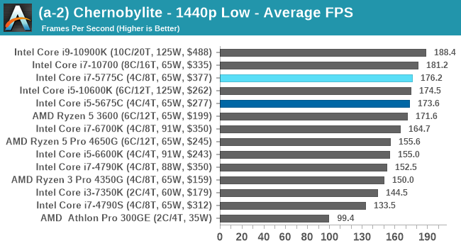
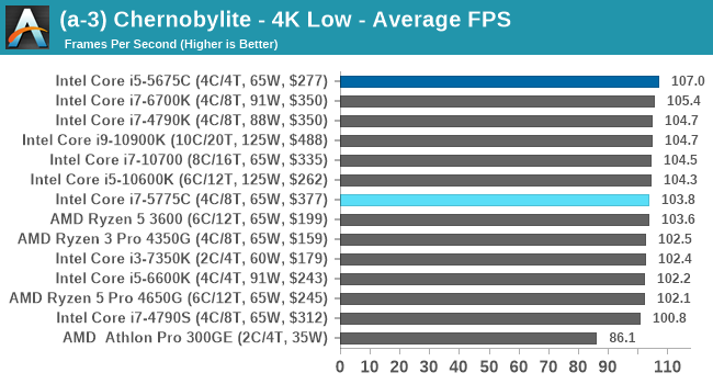
- 360p Low, 1440p Low, 4K Low, 1080p Max
We do as many runs within 10 minutes per resolution/setting combination, and then take averages.
| AnandTech | Low Res Low Qual |
Medium Res Low Qual |
High Res Low Qual |
Medium Res Max Qual |
| Average FPS | 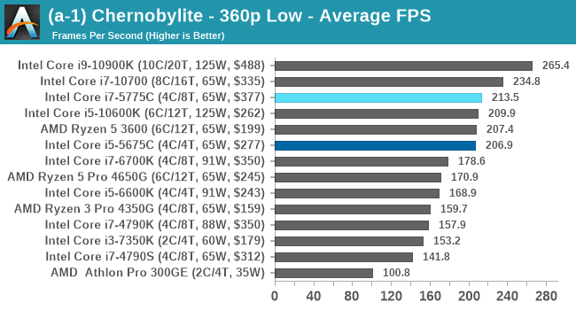 |
 |
 |
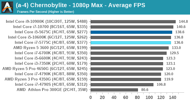 |
The Broadwell CPUs remain high performers here as the frame rates get cranked up, with the Broadwell Core i7+i5 even matching the latest Comet Lake Core i5, even at 1080p Max settings.
For our Integrated Tests, we run the first and last combination of settings.
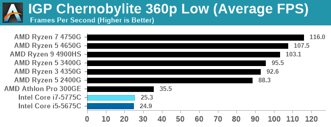
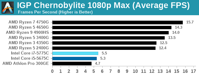
Integrated graphics shows how far AMD's basic options are ahead.


120 Comments
View All Comments
brucethemoose - Monday, November 2, 2020 - link
Is HBM2e access latency really lower than DDR4/5?I cant find any timing info or benchmarks, but my understanding is that its lower than GDDR6, which already has much higher latency than DDR4.
PeachNCream - Monday, November 2, 2020 - link
I'd like to say thanks for this review! I really love the look backwards at older hardware in relationship to modern systems. It really shows that in processor power terms that Broadwell/Haswell remain fairly relevant and the impact of eDRAM (or non-impact in various workloads) makes for really interesting reading.brucethemoose - Monday, November 2, 2020 - link
Another possibility: the "Radeon Cache" on an upcoming APU acts as a last level cache for the entire chip, just like Apple (and Qualcomm?) SoCs.Theres no extra packaging costs, no fancy 2nd chip, and it would save power.
Jorgp2 - Monday, November 2, 2020 - link
You do realize that Intel has had that about as long as they've had GPUs on their CPUs right?brucethemoose - Monday, November 2, 2020 - link
You mean the iGPUs share L3?Well, its wasn't a particularly large cache or powerful GPU until Broadwell came around.
Jorgp2 - Tuesday, November 3, 2020 - link
>Well, its wasn't a particularly large cache or powerful GPU until Broadwell came around.Larger than the caches on even AMDs largest GPUs until recently.
Hawaii had a 4MB cache, Vega had a 6MB I believe.
eastcoast_pete - Monday, November 2, 2020 - link
Thanks Ian, great article! Regarding a large, external L4 Cache: any guess on how speed and latency of eDRAM made in more modern silicon would compare with Broadwell's 22 nm one? Let's say if made in Intel's current 14 nm (++ etc)? And, if that'll speed it up enough to make it significantly better than current fast DDR4, would that be a way for Intel to put some "electronic nitrous" on its Tiger Lake and Rocket Lake chips? Because they do need something, or they'll get spanked badly by the new Ryzens.brucethemoose - Monday, November 2, 2020 - link
I'm guessing most of the latency comes from the travel between the chips, not from the speed of the eDRAM itself. So a shrink wouldnt help much, but EMIB might?There is talk of replacing on-chip SRAM in L3 cache with eDRAM, kind of like what IBM already does. So basically, its a size vs speed tradeoff, which is very interesting indeed.
quadibloc - Monday, November 2, 2020 - link
Well, AMD seems to think it was a good idea, given the 128 MB Infinity Cache on their latest graphics cards...Leeea - Monday, November 2, 2020 - link
Close, but not quite the same.AMD has their infinity cache in the GPU die. One piece of silicon for the whole thing. This may have faster I/O and less power consumption.
Intel's eDRAM caches were separate a separate piece of silicon all together.