A Broadwell Retrospective Review in 2020: Is eDRAM Still Worth It?
by Dr. Ian Cutress on November 2, 2020 11:00 AM ESTCPU Tests: Microbenchmarks
Core-to-Core Latency
As the core count of modern CPUs is growing, we are reaching a time when the time to access each core from a different core is no longer a constant. Even before the advent of heterogeneous SoC designs, processors built on large rings or meshes can have different latencies to access the nearest core compared to the furthest core. This rings true especially in multi-socket server environments.
But modern CPUs, even desktop and consumer CPUs, can have variable access latency to get to another core. For example, in the first generation Threadripper CPUs, we had four chips on the package, each with 8 threads, and each with a different core-to-core latency depending on if it was on-die or off-die. This gets more complex with products like Lakefield, which has two different communication buses depending on which core is talking to which.
If you are a regular reader of AnandTech’s CPU reviews, you will recognize our Core-to-Core latency test. It’s a great way to show exactly how groups of cores are laid out on the silicon. This is a custom in-house test built by Andrei, and we know there are competing tests out there, but we feel ours is the most accurate to how quick an access between two cores can happen.
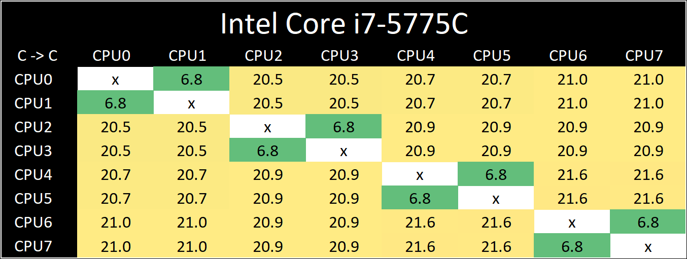
Broadwell is a familiar design, with all four cores connected in a ring-bus topology.
Cache-to-DRAM Latency
This is another in-house test built by Andrei, which showcases the access latency at all the points in the cache hierarchy for a single core. We start at 2 KiB, and probe the latency all the way through to 256 MB, which for most CPUs sits inside the DRAM (before you start saying 64-core TR has 256 MB of L3, it’s only 16 MB per core, so at 20 MB you are in DRAM).
Part of this test helps us understand the range of latencies for accessing a given level of cache, but also the transition between the cache levels gives insight into how different parts of the cache microarchitecture work, such as TLBs. As CPU microarchitects look at interesting and novel ways to design caches upon caches inside caches, this basic test proves to be very valuable.
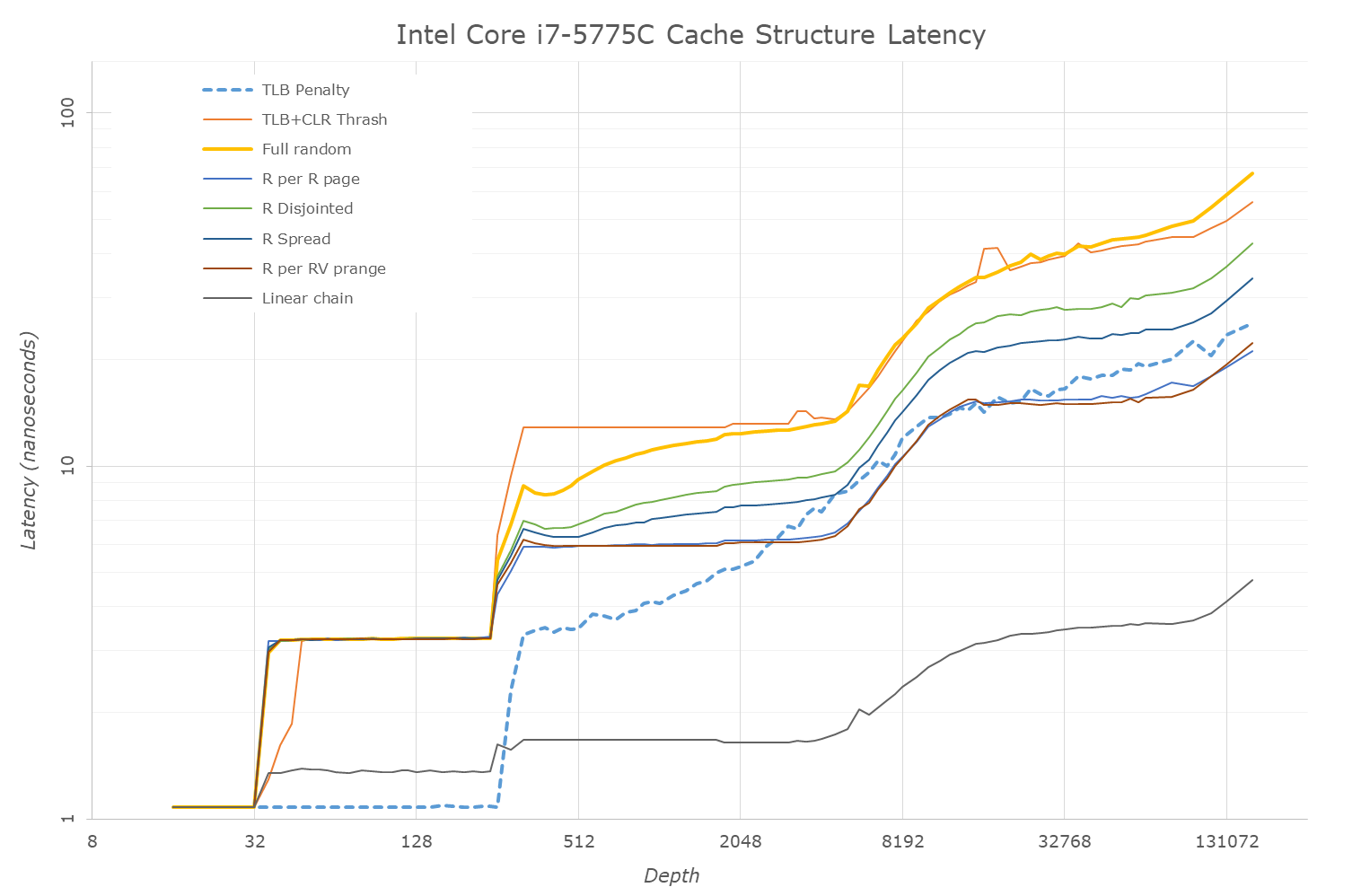
Our data shows a 4-cycle L1, a 12-cycle L2, a 26-50 cycle L3, while the eDRAM has a wide range from 50-150 cycles. This is still quicker than main memory, which goes to 200+ cycles.
Frequency Ramping
Both AMD and Intel over the past few years have introduced features to their processors that speed up the time from when a CPU moves from idle into a high powered state. The effect of this means that users can get peak performance quicker, but the biggest knock-on effect for this is with battery life in mobile devices, especially if a system can turbo up quick and turbo down quick, ensuring that it stays in the lowest and most efficient power state for as long as possible.
Intel’s technology is called SpeedShift, although SpeedShift was not enabled until Skylake.
One of the issues though with this technology is that sometimes the adjustments in frequency can be so fast, software cannot detect them. If the frequency is changing on the order of microseconds, but your software is only probing frequency in milliseconds (or seconds), then quick changes will be missed. Not only that, as an observer probing the frequency, you could be affecting the actual turbo performance. When the CPU is changing frequency, it essentially has to pause all compute while it aligns the frequency rate of the whole core.
We wrote an extensive review analysis piece on this, called ‘Reaching for Turbo: Aligning Perception with AMD’s Frequency Metrics’, due to an issue where users were not observing the peak turbo speeds for AMD’s processors.
We got around the issue by making the frequency probing the workload causing the turbo. The software is able to detect frequency adjustments on a microsecond scale, so we can see how well a system can get to those boost frequencies. Our Frequency Ramp tool has already been in use in a number of reviews.

From an idle frequency of 800 MHz, It takes ~32 ms for Intel to boost to 2.0 GHz, then another ~32 ms to get to 3.7 GHz. We’re essentially looking at 4 frames at 60 Hz to hit those high frequencies.
A y-Cruncher Sprint
The y-cruncher website has a large about of benchmark data showing how different CPUs perform to calculate specific values of pi. Below these there are a few CPUs where it shows the time to compute moving from 25 million digits to 50 million, 100 million, 250 million, and all the way up to 10 billion, to showcase how the performance scales with digits (assuming everything is in memory). This range of results, from 25 million to 250 billion, is something I’ve dubbed a ‘sprint’.
I have written some code in order to perform a sprint on every CPU we test. It detects the DRAM, works out the biggest value that can be calculated with that amount of memory, and works up from 25 million digits. For the tests that go up to the ~25 billion digits, it only adds an extra 15 minutes to the suite for an 8-core Ryzen CPU.
With this test, we can see the effect of increasing memory requirements on the workload and the scaling factor for a workload such as this.
- MT 25m: 1.617s
- MT 50m: 3.639s
- MT 100m: 8.156s
- MT 250m: 24.050s
- MT 500m: 53.525s
- MT 1000m: 118.651s
- MT 2500m: 341.330s
The scaling here isn’t linear – moving from 25m to 2.5b, we should see a 100x time increase, but instead it is 211x.


120 Comments
View All Comments
realbabilu - Monday, November 2, 2020 - link
That Larger cache maybe need specified optimized BLAS.Kurosaki - Monday, November 2, 2020 - link
Did you mean BIAS?ballsystemlord - Tuesday, November 3, 2020 - link
BLAS == Basic Linear Algebra System.Kamen Rider Blade - Monday, November 2, 2020 - link
I think there is merit to having Off-Die L4 cache.Imagine the low latency and high bandwidth you can get with shoving some stacks of HBM2 or DDR-5, whichever is more affordable and can better use the bandwidth over whatever link you're providing.
nandnandnand - Monday, November 2, 2020 - link
I'm assuming that Zen 4 will add at least 2-4 GB of L4 cache stacked on the I/O die.ichaya - Monday, November 2, 2020 - link
Waiting for this to happen... have been since TR1.nandnandnand - Monday, November 2, 2020 - link
Throw in an RDNA 3 chiplet (in Ryzen 6950X/6900X/whatever) for iGPU and machine learning, and things will get really interesting.ichaya - Monday, November 2, 2020 - link
Yep.dotjaz - Saturday, November 7, 2020 - link
That's definitely not happening. You are delusional if you think RDNA3 will appear as iGPU first.At best we can hope the next I/O die to intergrate full VCN/DCN with a few RDNA2 CUs.
dotjaz - Saturday, November 7, 2020 - link
Also doubly delusional if think think RDNA3 is any good for ML. CDNA2 is designed for that.Adding powerful iGPU to Ryzen 9 servers literally no purpose. Nobody will be satisfied with that tiny performance. Guaranteed recipe for instant failure.
The only iGPU that would make sense is a mini iGPU in I/O die for desktop/video decoding OR iGPU coupled with low end CPU for an complete entry level gaming SOC aka APU. Chiplet design almost makes no sense for APU as long as GloFo is in play.