The Intel Xe-LP GPU Architecture Deep Dive: Building Up The Next Generation
by Ryan Smith on August 13, 2020 9:00 AM EST- Posted in
- GPUs
- Intel
- Tiger Lake
- Xe
- Xe-LP
- DG1
- Intel Arch Day 2020
- SG1
Feed the Beast: New L1 Cache & Dual Ring Buses
Shifting gears, let’s take a look at the memory subsystem for Xe-LP and how Intel will be feeding the beast that is their new GPU architecture. Among many contemporary firsts for Intel’s GPU architectures, Xe-LP will find itself in the interesting position of straddling the line between an integrated GPU and a discrete GPU. Which is to say that it has to be able to work with both Tiger Lake’s shared IMC, as well as DG1’s own dedicated memory controller.
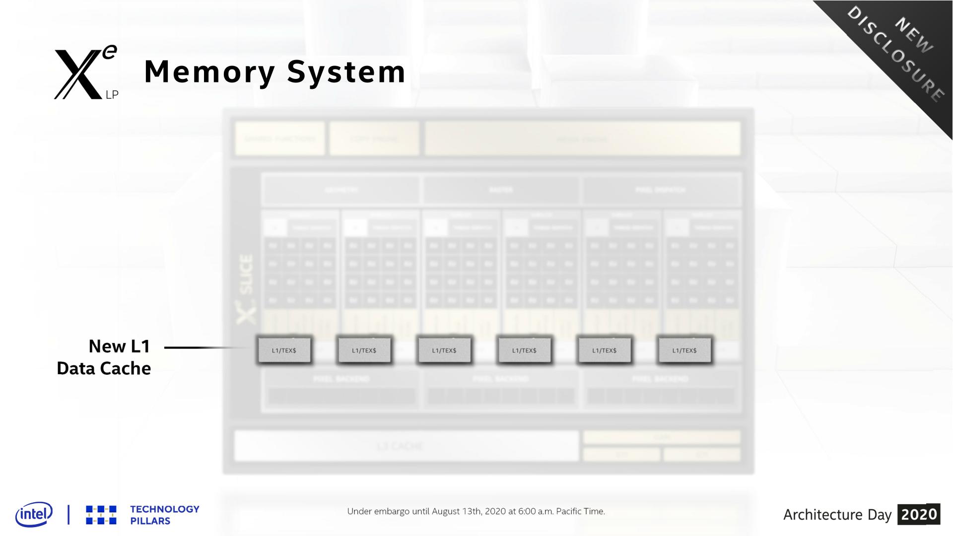
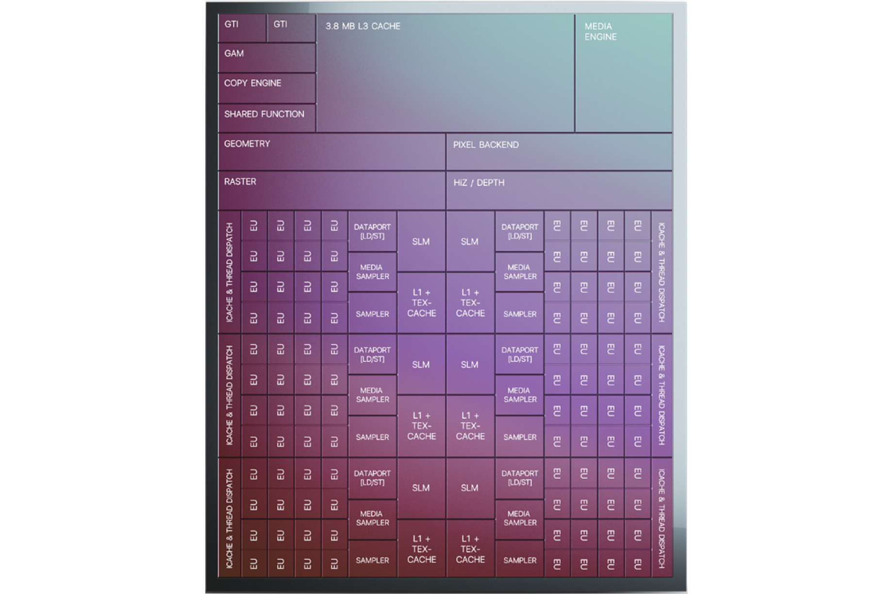
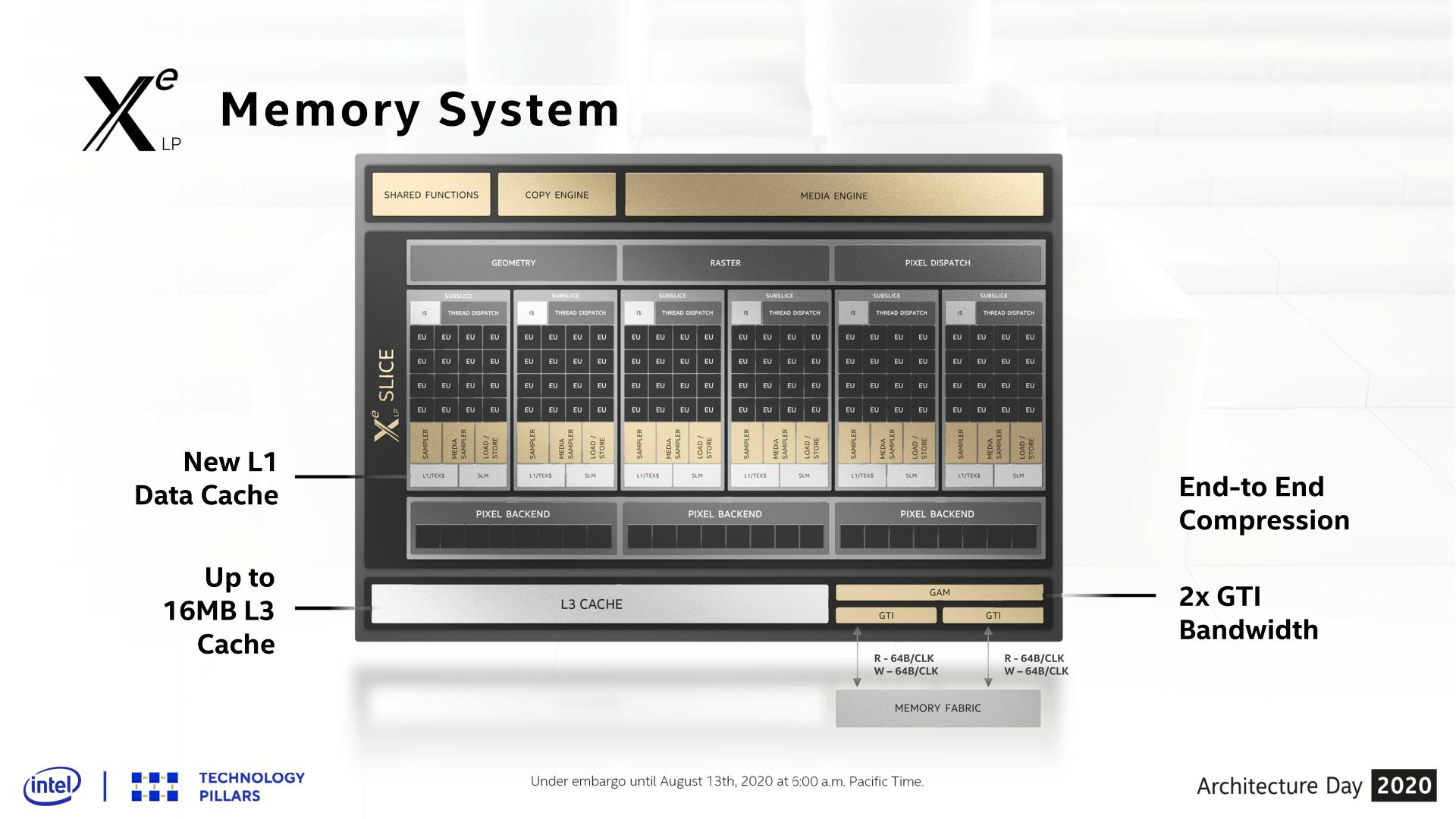
Starting with the subslices, Xe-LP introduces a new combined L1 data and texture cache. Information about this cache is limited, but Intel has confirmed that it’s a 64KB per subslice cache, and that it can be dynamically reconfigured between L1 and texture caching as necessary. According to the company, they added the L1 cache as a result of their workload analysis, and that doing so improved the performance of the load/store pipeline. Unfortunately, it’s not clear how this fits into the bigger picture with Intel’s previous subslice L2 cache, and whether that’s been replaced or still exists and is merely not on these diagrams.
The on-GPU L3 cache (not to be confused with Tiger Lake’s shared Last Level Cache) has also undergone its own upgrades, receiving both a capacity and a bandwidth boost. On the capacity front, the L3 cache can now be as large as 16MB, as opposed to just 3MB on Gen11. That said, based on Intel’s Tiger Lake disclosures, it’s clear that such a large cache isn’t coming to Intel’s SoCs; instead Tiger Lake will ship with a 3.8MB GPU L3 cache. Tiger Lake has its own LLC beyond this, which the GPU can tap into as well, so it doesn’t necessarily need quite such a large cache.
For DG1, on the other hand, the GPU’s L3 cache is the last caching level, so a larger cache makes practical sense there. To that end I wouldn’t be surprised if that’s exactly what we see on DG1: a 16MB L3 cache. Though Intel has reiterated that this is an architectural presentation and not a product presentation, so it may very well be that they aren’t outfitting any Xe-LP GPUs with a max size L3 cache.
This larger L3 cache is also faster than Gen11’s L3, with Intel doubling the transfer size. Xe-LP’s L3 cache can now transfer 128 bytes/clock, which for a theoretical 1.6GHz chip would give it over 190GB/sec of internal L3 bandwidth. This upgrade is important for feeding the ROPs and other parts of the GPU, and goes hand-in-hand with Intel’s goal to double GPU performance, which means they need to feed the beast a lot more data in the process. Plus this change also keeps the L3 cache aligned with what the new dual ringbus can do.
One of the more enigmatic changes for Tiger Lake, the SoC has added a second, seemingly identical ringbus to the chip, creating a second loop that connects the four CPU cores and the iGPU to the integrated memory controller. As a consequence of this, the iGPU now needs two Graphics Technology Interface (GTI) ports to create the two ringbus stops.
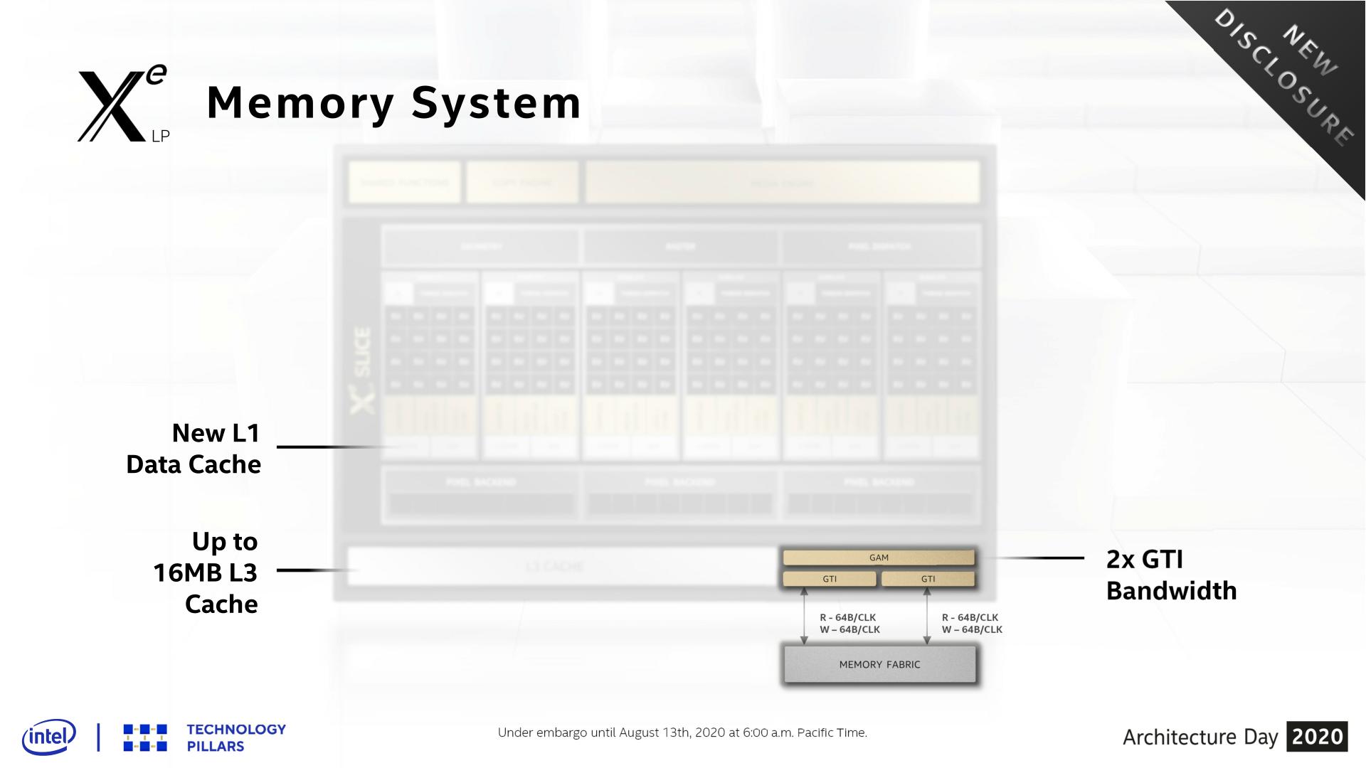
The big benefit of this change is that, all other aspects held equal, this doubles the amount of bandwidth between the GPU and the IMC on Tiger Lake. So instead of only being able to transfer 64B/clock up and down, Xe-LP on Tiger Lake can send two 64B requests (for a total of 128B/clock) using the two ringbuses.
Given that at this juncture the iGPU has become the largest consumer of bandwidth on an Intel SoC, I strongly suspect that the second ringbus has been added primarily for the iGPU’s benefit. Unfortunately this isn’t something we can directly math out, as the ringbus having its own clock domain complicates matters a bit, so it’s not clear if 1 ringbus can even match the memory bandwidth of a Tiger Lake chip with LPDDR5-5200. But even if it can, the an even higher performing GPU like Xe-LP is no doubt putting a good deal of pressure on Intel’s SoC memory subsystem.
Meanwhile this also gives us a very strong hint that DG1 will utilize a 128-bit memory bus for its dedicated VRAM. The 2x64B backend could very easily be hooked up to a 128-bit memory controller, instead of the two 64B ringbuses. This would also ensure that DG1 gets as much or more memory bandwidth than Tiger Lake – and with the bonus of not having to share it with other parts of the system.
Finally, even with the significant bandwidth improvements underneath, Intel has also been working to reduce their bandwidth consumption. Xe-LP ships with updated versions of their color and depth compression algorithms, which although Intel isn’t providing specific figures for it, any improvements here will directly translate into reduced memory traffic. Meanwhile the company is also extending this compression functionality to the media and display interfaces, which means that image data can stay compressed whenever it’s being moved between the graphics engine, the media engine, and the display.


33 Comments
View All Comments
Cooe - Saturday, August 15, 2020 - link
Soooooo much die space & transistors needed for just barely better performance than Renoir's absolutely freaking MINISCULE Vega 8 iGPU block.... Consider me seriously unimpressed. The suuuuuper early DDR5 support on the IMC is incredibly intriguing and I'm really curious to see what the performance gains from that will be like, but other than that.... epic yawn. Wake me up when it doesn't take Intel half the damn die for them to compete with absolutely teeny-tiny implementations of AMD's 2-3 year old GPU tech....Makes sense now why AMD's going for Vega again for Cézanne. Some extra frequency & arch tweaks are all they'd need to one-up Intel again, & going RDNA/2 would have had a SIGNIFICANTLY larger die space requirement (an RDNA dCU ["Dual Compute Unit"] is much, MUCH larger than 2x Vega II /"Enhanced" CU's), that just doesn't really make much sense to make until DDR5 shows up with Zen 4 and such a change can be properly taken advantage of.
(Current iGPU's are ALREADY ridiculously memory bandwidth bottlenecked. A beefy RDNA 2 iGPU block would bring even 3200MHz DDR4 to its absolute KNEES, & LPDDR4X is just too uncommon/expensive to bank on it being used widely enough for the huge die space cost vs iterating Vega again to make sense. Also, as we saw with Renoir; with some additional TLC, Vega has had a LOT more left in the tank than probably anyone of us would have thought).
Oxford Guy - Tuesday, August 18, 2020 - link
MadTV is back, with an episode called Anandtech Literally?Oxford Guy - Tuesday, August 18, 2020 - link
"t’s worth noting that this change is fairly similar to what AMD did last year with its RDNA (1) architecture, eliminating the multi-cycle execution of a wavefront by increasing their SIMD size and returning their wavefront size. In AMD’s case this was done to help keep their SIMD slots occupied more often and reduce instruction latency, and I wouldn’t be surprised if it’s a similar story for Intel."Retuning or returning to?