AMD Rome Second Generation EPYC Review: 2x 64-core Benchmarked
by Johan De Gelas on August 7, 2019 7:00 PM ESTMemory Subsystem: TinyMemBench
We doublechecked our LMBench numbers with Andrei's custom memory latency test.
The latency tool also measures bandwidth and it became clear than once we move beyond 16 MB, DRAM is accessed. When Andrei compared with our Ryzen 9 3900x numbers, he noted:
The prefetchers on the Rome platform don't look nearly as aggressive as on the Ryzen unit on the L2 and L3
It would appear that parts of the prefetchers are adjusted for Rome compared to Ryzen 3000. In effect, the prefetchers are less aggressive than on the consumer parts, and we believe that AMD has made this choice by the fact that quite a few applications (Java and HPC) suffer a bit if the prefetchers take up too much bandwidth. By making the prefetchers less aggressive in Rome, it could aid performance in those tests.
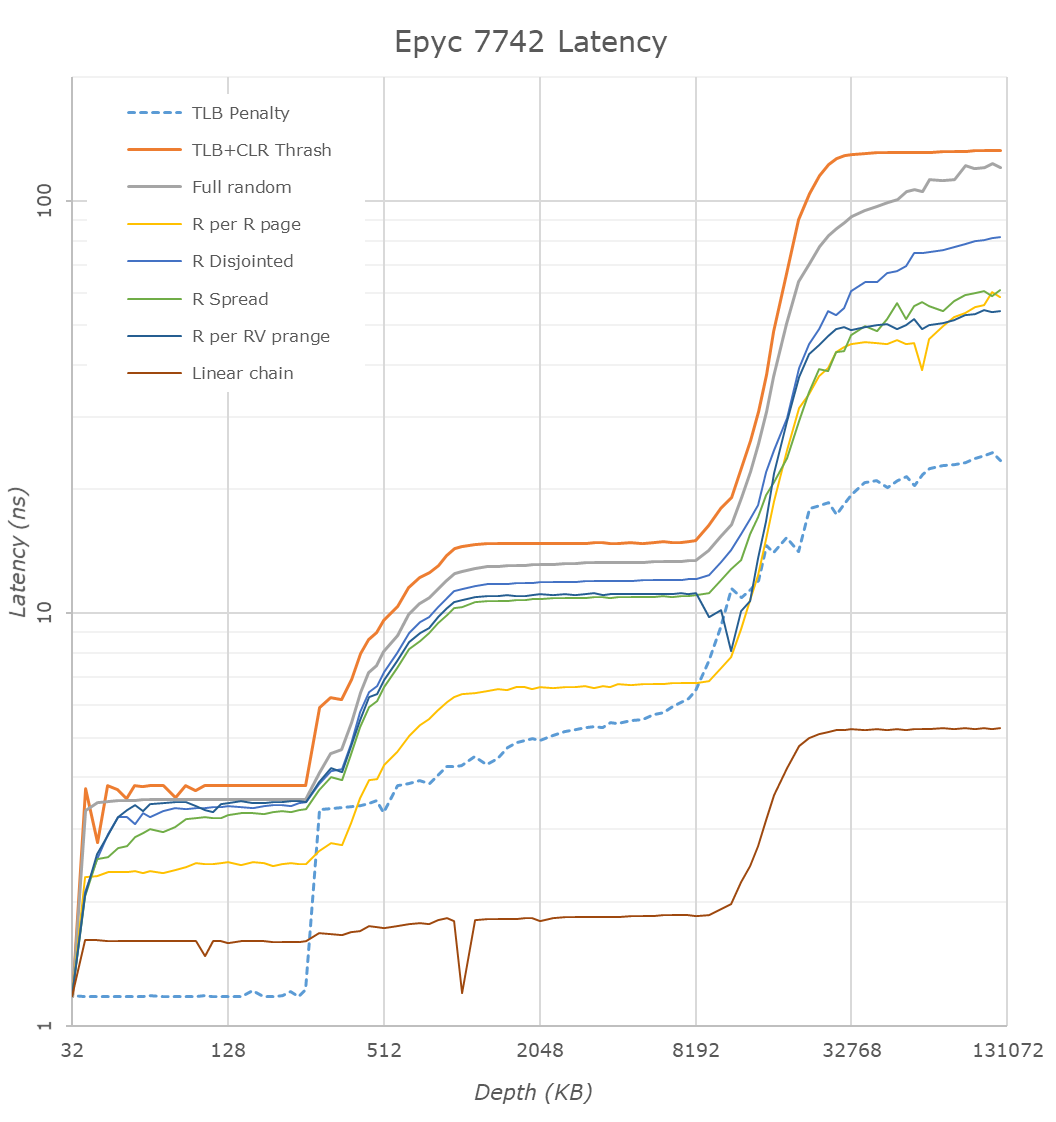
While we could not retest all our servers with Andrei's memory latency test by the deadline (see the "Murphy's Law" section on page 5), we turned to our open source TinyMemBench benchmark results. The source was compiled for x86 with GCC and the optimization level was set to "-O3". The measurement is described well by the manual of TinyMemBench:
Average time is measured for random memory accesses in the buffers of different sizes. The larger the buffer, the more significant the relative contributions of TLB, L1/L2 cache misses, and DRAM accesses become. All the numbers represent extra time, which needs to be added to L1 cache latency (4 cycles).
We tested with dual random read, as we wanted to see how the memory system coped with multiple read requests.
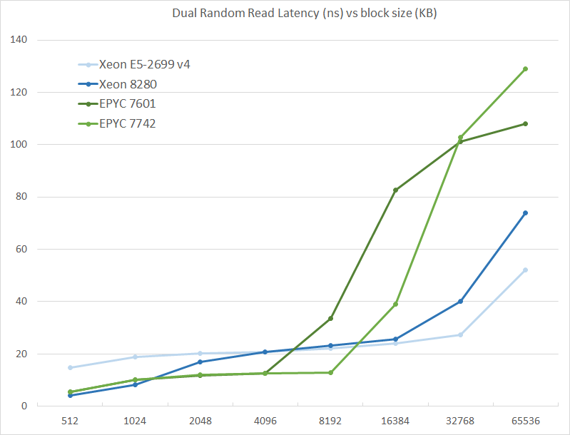
The graph shows how the larger L3 cache of the EPYC 7742 resulting in a much lower latency between 4 and 16 MB, compared to the EPYC 7601. The L3 cache inside the CCX is also very fast (2-8 MB) compared to Intel's Mesh (8280) and Ring topologies (E5).
However, once we access more than 16 MB, Intel has a clear advantage due to the slower but much larger shared L3 cache. When we tested the new EPYC CPUs in a more advanced NUMA setting (with NPS = 4 setting, meaning 4 nodes per socket), latency at 64 MB lowered from 129 to 119. We quote AMD's engineering:
In NPS4, the NUMA domains are reported to software in such a way as it chiplets always access the near (2 channels) DRAM. In NPS1 the 8ch are hardware-interleaved and there is more latency to get to further ones. It varies by pairs of DRAM channels, with the furthest one being ~20-25ns (depending on the various speeds) further away than the nearest. Generally, the latencies are +~6-8ns, +~8-10ns, +~20-25ns in pairs of channels vs the physically nearest ones."
So that also explains why AMD states that select workloads achieve better performance with NPS = 4.


180 Comments
View All Comments
ET - Thursday, August 8, 2019 - link
I found the EPYC 7262 the most interesting SKU. By L3 cache size, that would be 4 chiplets, each offering only 2 cores. From the specs it looks like AMD has no shortage of 4 core chiplets, but I didn't expect 2 core chiplets.Rudde - Friday, August 9, 2019 - link
L3 cache is shared inside a CCX (4 cores), which suggests that every CCX has only one core available, but 16MB of L3 cache. I.e. every core has private L3 cache.colonelclaw - Thursday, August 8, 2019 - link
But can it serve Crysis Battle Royale?shing3232 - Thursday, August 8, 2019 - link
I am pretty sure it can lolBigMamaInHouse - Thursday, August 8, 2019 - link
@ Johan De Gelas will u test @240W TDP config?JohanAnandtech - Thursday, August 8, 2019 - link
Elaborate your interest in that, as it is only tad higher than the official 225W TDP?BigMamaInHouse - Thursday, August 8, 2019 - link
AMD is offering 225W/240W TDP option in bios to it's customers and lets them to decide if to go with better cooling and use 240W or stay at 225W, even though it looks small increase- in reality it should offer almost 10% more power headroom to the CPU chiplets -if you consider that the 225W is including ~55W for I/O die, so extra 15W for the chiplets alone should offer nice bump in clocks.Gondalf - Thursday, August 8, 2019 - link
Strange.....the article forgot Cooper Lake, out in Q4 this year and at major customers (for revenue) from at least two quarters. Same applies to Ice Lake SP that is in evaluation to OEMs right now.From the article looks like Intel is sleeping, but it is not at all. Ummm maybe Intel is snobbing some guys here not giving samples to test?? or informations to share??
Bet Intel have to argue about the test suite or about compiler settings.........
JohanAnandtech - Thursday, August 8, 2019 - link
Because Cooper Lake is still "warmed up Skylake" (unless I missed something). AFAIK it is Cascade Lake with 8 mem channels - so the 56-core socketed will probably be still in the 350-400W TDP range. So the SPEC benchmarks will look better, but getting that kind of server running inside your datacenter does not look very attractive: complex and thus expensive boards, high cooling and power distribution required. Looks like a chip that wins back benchmarks, but is too much hassle to roll out in high quantities.Null666666 - Friday, August 9, 2019 - link
Wondering when 4-8 socket ice lake is due.