AMD Zen 2 Microarchitecture Analysis: Ryzen 3000 and EPYC Rome
by Dr. Ian Cutress on June 10, 2019 7:22 PM EST- Posted in
- CPUs
- AMD
- Ryzen
- EPYC
- Infinity Fabric
- PCIe 4.0
- Zen 2
- Rome
- Ryzen 3000
- Ryzen 3rd Gen
New Instructions
Cache and Memory Bandwidth QoS Control
As with most new x86 microarchitectures, there is a drive to increase performance through new instructions, but also try for parity between different vendors in what instructions are supported. For Zen 2, while AMD is not catering to some of the more exotic instruction sets that Intel might do, it is adding in new instructions in three different areas.
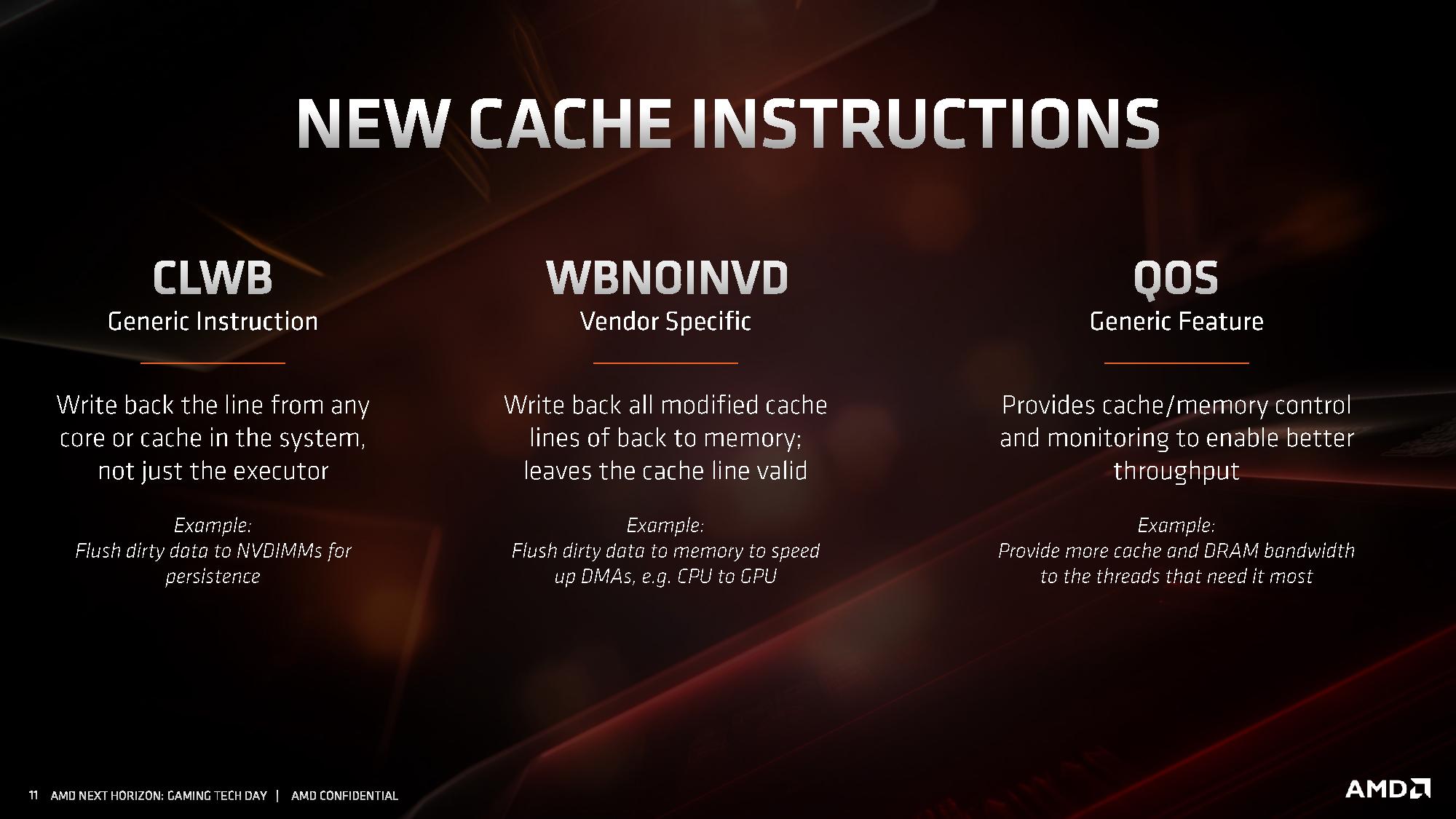
The first one, CLWB, has been seen before from Intel processors in relation to non-volatile memory. This instruction allows the program to push data back into the non-volatile memory, just in case the system receives a halting command and data might be lost. There are other instructions associated with securing data to non-volatile memory systems, although this wasn’t explicitly commented on by AMD. It could be an indication that AMD is looking to better support non-volatile memory hardware and structures in future designs, particularly in its EPYC processors.
The second cache instruction, WBNOINVD, is an AMD-only command, but builds on other similar commands such as WBINVD. This command is designed to predict when particular parts of the cache might be needed in the future, and clears them up ready in order to accelerate future calculations. In the event that the cache line needed isn’t ready, a flush command would be processed in advance of the needed operation, increasing latency – by running a cache line flush in advance while the latency-critical instruction is still coming down the pipe helps accelerate its ultimate execution.
The final set of instructions, filed under QoS, actually relates to how cache and memory priorities are assigned.
When a cloud CPU is split into different containers or VMs for different customers, the level of performance is not always consistent as performance could be limited based on what another VM is doing on the system. This is known as the ‘noisy neighbor’ issue: if someone else is eating all the core-to-memory bandwidth, or L3 cache, it can be very difficult for another VM on the system to have access to what it needs. As a result of that noisy neighbor, the other VM will have a highly variable latency on how it can process its workload. Alternatively, if a mission critical VM is on a system and another VM keeps asking for resources, the mission critical one might end up missing its targets as it doesn’t have all the resources it needs access to.
Dealing with noisy neighbors, beyond ensuring full access to the hardware as a single user, is difficult. Most cloud providers and operations won’t even tell you if you have any neighbors, and in the event of live VM migration, those neighbors might change very frequently, so there is no guarantee of sustained performance at any time. This is where a set of dedicated QoS (Quality of Service) instructions come in.
As with Intel’s implementation, when a series of VMs is allocated onto a system on top of a hypervisor, the hypervisor can control how much memory bandwidth and cache that each VM has access to. If a mission critical 8-core VM requires access to 64 MB of L3 and at least 30 GB/s of memory bandwidth, the hypervisor can control that the priority VM will always have access to that amount, and either eliminate it entirely from the pool for other VMs, or intelligently restrict the requirements as the mission critical VM bursts into full access.
Intel only enables this feature on its Xeon Scalable processors, however AMD will enable it up and down its Zen 2 processor family range, for consumers and enterprise users.
The immediate issue I had with this feature is on the consumer side. Imagine if a video game demands access to all the cache and all the memory bandwidth, while some streaming software would get access to none – it could cause havoc on the system. AMD explained that while technically individual programs can request a certain level of QoS, however it will be up to the OS or the hypervisor to control if those requests are both valid and suitable. They see this feature more as an enterprise feature used when hypervisors are in play, rather than bare metal installations on consumer systems.


216 Comments
View All Comments
Walkeer - Thursday, June 13, 2019 - link
Superb analysis, thanks a lot @Ian! very excited to have the 3900x at home alreadyFreckledTrout - Thursday, June 13, 2019 - link
Reading over the Zen2 microarchitecture article Im left wondering if the Windows scheduler improvements are making use of a new unmentioned RDPID feature in Zen2 to determine where threads are placed?cooker358 - Thursday, June 13, 2019 - link
感谢分享!Gastec - Thursday, June 13, 2019 - link
I too am curious about the latencies, particularly between the chiplets. With the clock selection down to 2 ns and Windows' 10 hopefully improved thread allocation (filling a CCX, then the next one before jumping to the 2nd chiplet) latencies should be lower. We'll just have to wait for honest extensive testing and reviews to be done. You were not planning on buying these CPUs on release day or even worse, pre-ordering them, were you? :)jamescox - Sunday, June 16, 2019 - link
I expect the CCX to CCX latencies to be very good. There is no memory clock on the cpu chiplet, so the two on die CCX almost certainly communicate at cpu clock rather than memory clock as in Zen 1. It isn’t the same as Intel’s mesh network, but AMD’s solution will have better L3 latency within the CCX compared to Intel. Intel’s mesh network seems to be terrible for power consumption. Intel’s ring bus didn’t scale to enough cores. For their 18 core chip (if I am remembering right), they actually had 3 separate ring buses. The mesh network is obviously not workable across multiple chiplets, so it will be interesting to see what Intel does.For the chiplet to chiplet latency, they have more than doubled the infinity fabric serdes clock with the higher than PCIe 4.0 speeds. It seems that the internal IF clock is also around doubled. It was operating at actual memory clock in Sen 1 which was half the DDR rate. They seem to be running the internal IF clock the same as the DDR rate with the option to drop back to half DDR rate. So if you are running DDR 3200, the IF clock may actually be 3200 instead of 1600 as it would be in Zen 1. If you re overclocking to DDR 4000 or something, then it may need to drop down to 2000 for the internal IF clock. If this is the way it is set up, then they may have an option to explicitly set the divider, but it is probably going to not be stable past 3.7 GHz or so. The IO die is 14 nm global foundries, so that seems like a reasonable limitation.
The CCX to CCX latency should be less important as the OS and software is better optimized for the architecture. There was quite a few cases on Zen 1 of applications performing significantly better on Linux compared to windows due to the scheduler. Most applications can be optimized a bit for this architecture also. The problem is fine grained shared memory between threads on different CCX. It generally a good idea to reduce that anyway since locking can be detrimental to performance. With Zen 2, I think application level optimizations are probably going to be a lot less necessary anyway, but a lot of the early issues were probably caused by bad multi-threaded programming. This type of architecture isn’t going away. Intel can’t compete with Epyc 2 with a monolithic die. Epyc 2 will be around 1000 square mm of silicon total. Intel can’t scale core count without moving to something similar.
frshi - Friday, June 14, 2019 - link
@Ian Cutress What about 2x16GB sticks compared to 4x8GB? I remember Zen and Zen+ were kinda picky when using 4 sticks. Any change to that on Zen 2?RAINFIRE - Saturday, June 15, 2019 - link
Yeah - I'm curious. Can anyone speak to the (4 x 32GB) memory that Ryzen 3000 and x570 boards are supposed to support?Holliday75 - Wednesday, June 19, 2019 - link
IF reviewers have samples at this time they are under an NDA until July 7th. Only unconfirmed leaks can provide that kind of info and its super early. A lot of these types of issues won't be known until they go retail.AdrianMel - Sunday, June 16, 2019 - link
I would like these AMD chips to be used on laptops. Would be a breakthrough in terms of computing power, lower consumption. I think if a HBM2 or higher memory is integrated into the processor, I think it will double the computing power. Ar fi de studiat si o implementare a 2 porturi superiare thnic vechiului expresscard 54 in care sa putem introduce in laptopuri 2 placi videojamescox - Sunday, June 16, 2019 - link
Everyone keeps bringing up HBM for cpus as if it is magical in some manner. HBM can provide high bandwidth, but it is still DRAM. He latency isn’t that great, so it isn’t really that useful as a cpu cache. If you are trying to run AVX512 code across a bunch of CPU cores, then maybe you could use the bandwidth. If you have code that can use that level of parallelism, then it will almost certainly run much more efficiently on an actual gpu. I didn’t think that expanding AVX to 512-bits was a good idea. There isn’t too much difference from a cpu perspective between 1 512-bit instruction and 2 256-bit instructions. The registers are wider, but they can have many more smaller registers that are specified in the ISA by using existing register renaming techniques. At 14 nm, the 512-bit units seem to take too much space and consume too much power. They may be more easily doable in 7 nm or below eventually, but they may still have issues running at cpu core clocks. If you have to run it at half clock (which is about where gpus are vs. cpus) then you have lost the advantage of going double the width anyway. IMO, the AVX 512 instructions were Intel’s failed attempt (Xeon Phi seems to have been a disappointment) at making a cpu act like a gpu. They have basically given that up and are now designing an actual gpu.I went off in a bit of a tangent there, but HBM really isn’t that useful for a cpu cache. It isn’t going to be that low of latency; so it would not increase single thread performance much compared to stuff actually designed to be a low latency cache. The next generations form AMD May start using active silicon interposers, but I would doubt that they would use HBM. The interposer is most likely to be used in place of the IO die. They could place all of the large transistors needed for driving off die interfaces (reason why IO doesn’t scale well) in the active interposer. They could then stack 7 nm chips on top of the active interposer for the actual logic. Cache scales very well which is why AMD can do a $200 chip with 32 MB of L3 cache and a $500 chip with 64 MB of L3. Intel 14 nm chips top out at 38.5 MB, mostly for high priced Xeon chips. With an active interposer, they could, for example) make something like 4 or 8 memory controller chips with large SRAM caches on 7 nm while using the active interposer for the IO drivers. Many different configurations are possible with an active interposer, so it is hard to speculate. Placing HBM on the IO interposer, as the AdoredTV guy has speculated, doesn’t sound like a great idea. Two stacks of HBM deliver 512 GB/s, which would take around 10 IF links to transfer to the CPU chiplets. That would be a massive waste of power. If they do use HBM for cpu chiplets, you would want to connect it directly to the cpu chiplet; you would place the a cpu chiplet and HBM stack on the same interposer. That would have some latency advantage, but mostly for large systems like Epyc.