AMD Zen 2 Microarchitecture Analysis: Ryzen 3000 and EPYC Rome
by Dr. Ian Cutress on June 10, 2019 7:22 PM EST- Posted in
- CPUs
- AMD
- Ryzen
- EPYC
- Infinity Fabric
- PCIe 4.0
- Zen 2
- Rome
- Ryzen 3000
- Ryzen 3rd Gen
Windows Optimizations
One of the key points that have been a pain in the side of non-Intel processors using Windows has been the optimizations and scheduler arrangements in the operating system. We’ve seen in the past how Windows has not been kind to non-Intel microarchitecture layouts, such as AMD’s previous module design in Bulldozer, the Qualcomm hybrid CPU strategy with Windows on Snapdragon, and more recently with multi-die arrangements on Threadripper that introduce different memory latency domains into consumer computing.
Obviously AMD has a close relationship with Microsoft when it comes down to identifying a non-regular core topology with a processor, and the two companies work towards ensuring that thread and memory assignments, absent of program driven direction, attempt to make the most out of the system. With the May 10th update to Windows, some additional features have been put in place to get the most out of the upcoming Zen 2 microarchitecture and Ryzen 3000 silicon layouts.
The optimizations come on two fronts, both of which are reasonably easy to explain.
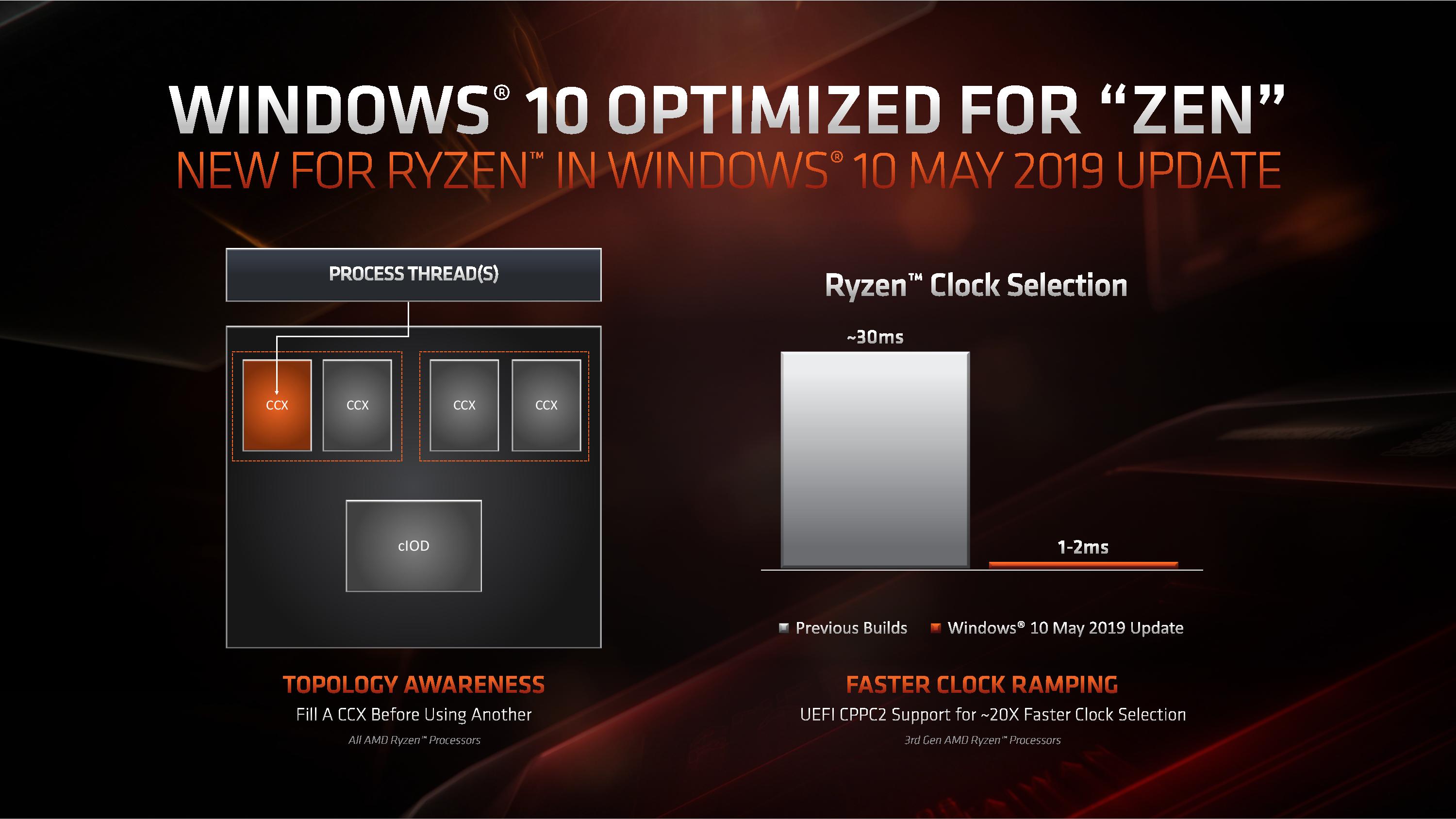
Thread Grouping
The first is thread allocation. When a processor has different ‘groups’ of CPU cores, there are different ways in which threads are allocated, all of which have pros and cons. The two extremes for thread allocation come down to thread grouping and thread expansion.
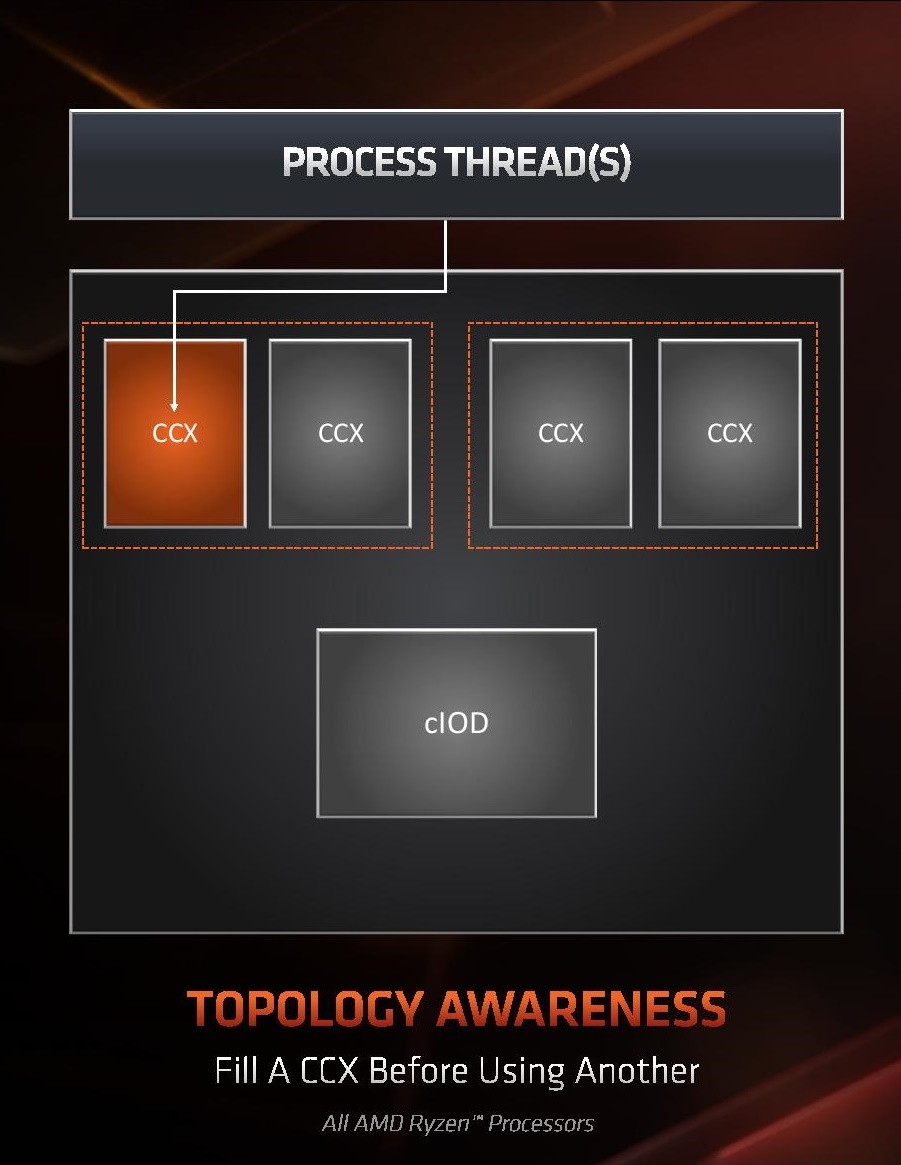
Thread grouping is where as new threads are spawned, they will be allocated onto cores directly next to cores that already have threads. This keeps the threads close together, for thread-to-thread communication, however it can create regions of high power density, especially when there are many cores on the processor but only a couple are active.
Thread expansion is where cores are placed as far away from each other as possible. In AMD’s case, this would mean a second thread spawning on a different chiplet, or a different core complex/CCX, as far away as possible. This allows the CPU to maintain high performance by not having regions of high power density, typically providing the best turbo performance across multiple threads.
The danger of thread expansion is when a program spawns two threads that end up on different sides of the CPU. In Threadripper, this could even mean that the second thread was on a part of the CPU that had a long memory latency, causing an imbalance in the potential performance between the two threads, even though the cores those threads were on would have been at the higher turbo frequency.
Because of how modern software, and in particular video games, are now spawning multiple threads rather than relying on a single thread, and those threads need to talk to each other, AMD is moving from a hybrid thread expansion technique to a thread grouping technique. This means that one CCX will fill up with threads before another CCX is even accessed. AMD believes that despite the potential for high power density within a chiplet, while the other might be inactive, is still worth it for overall performance.
For Matisse, this should afford a nice improvement for limited thread scenarios, and on the face of the technology, gaming. It will be interesting to see how much of an affect this has on the upcoming EPYC Rome CPUs or future Threadripper designs. The single benchmark AMD provided in its explanation was Rocket League at 1080p Low, which reported a +15% frame rate gain.
Clock Ramping
For any of our users familiar with our Skylake microarchitecture deep dive, you may remember that Intel introduced a new feature called Speed Shift that enabled the processor to adjust between different P-states more freely, as well as ramping from idle to load very quickly – from 100 ms to 40ms in the first version in Skylake, then down to 15 ms with Kaby Lake. It did this by handing P-state control back from the OS to the processor, which reacted based on instruction throughput and request. With Zen 2, AMD is now enabling the same feature.

AMD already has sufficiently more granularity in its frequency adjustments over Intel, allowing for 25 MHz differences rather than 100 MHz differences, however enabling a faster ramp-to-load frequency jump is going to help AMD when it comes to very burst-driven workloads, such as WebXPRT (Intel’s favorite for this sort of demonstration). According to AMD, the way that this has been implemented with Zen 2 will require BIOS updates as well as moving to the Windows May 10th update, but it will reduce frequency ramping from ~30 milliseconds on Zen to ~1-2 milliseconds on Zen 2. It should be noted that this is much faster than the numbers Intel tends to provide.
The technical name for AMD’s implementation involves CPPC2, or Collaborative Power Performance Control 2, and AMD’s metrics state that this can increase burst workloads and also application loading. AMD cites a +6% performance gain in application launch times using PCMark10’s app launch sub-test.
Hardened Security for Zen 2
Another aspect to Zen 2 is AMD’s approach to heightened security requirements of modern processors. As has been reported, a good number of the recent array of side channel exploits do not affect AMD processors, primarily because of how AMD manages its TLB buffers that have always required additional security checks before most of this became an issue. Nonetheless, for the issues to which AMD is vulnerable, it has implemented a full hardware-based security platform for them.
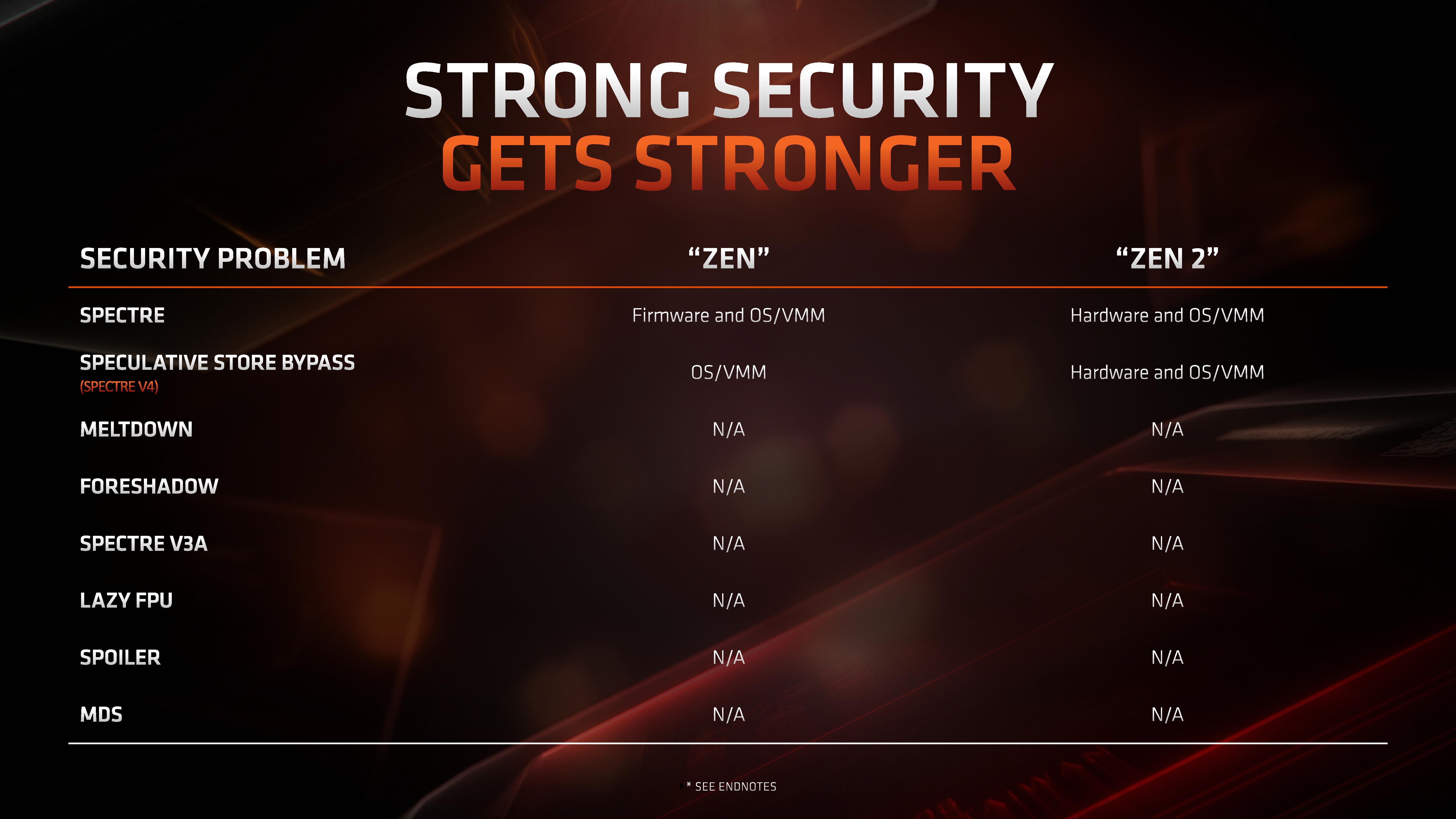
The change here comes for the Speculative Store Bypass, known as Spectre v4, which AMD now has additional hardware to work in conjunction with the OS or virtual memory managers such as hypervisors in order to control. AMD doesn’t expect any performance change from these updates. Newer issues such as Foreshadow and Zombieload do not affect AMD processors.


216 Comments
View All Comments
Walkeer - Thursday, June 13, 2019 - link
Superb analysis, thanks a lot @Ian! very excited to have the 3900x at home alreadyFreckledTrout - Thursday, June 13, 2019 - link
Reading over the Zen2 microarchitecture article Im left wondering if the Windows scheduler improvements are making use of a new unmentioned RDPID feature in Zen2 to determine where threads are placed?cooker358 - Thursday, June 13, 2019 - link
感谢分享!Gastec - Thursday, June 13, 2019 - link
I too am curious about the latencies, particularly between the chiplets. With the clock selection down to 2 ns and Windows' 10 hopefully improved thread allocation (filling a CCX, then the next one before jumping to the 2nd chiplet) latencies should be lower. We'll just have to wait for honest extensive testing and reviews to be done. You were not planning on buying these CPUs on release day or even worse, pre-ordering them, were you? :)jamescox - Sunday, June 16, 2019 - link
I expect the CCX to CCX latencies to be very good. There is no memory clock on the cpu chiplet, so the two on die CCX almost certainly communicate at cpu clock rather than memory clock as in Zen 1. It isn’t the same as Intel’s mesh network, but AMD’s solution will have better L3 latency within the CCX compared to Intel. Intel’s mesh network seems to be terrible for power consumption. Intel’s ring bus didn’t scale to enough cores. For their 18 core chip (if I am remembering right), they actually had 3 separate ring buses. The mesh network is obviously not workable across multiple chiplets, so it will be interesting to see what Intel does.For the chiplet to chiplet latency, they have more than doubled the infinity fabric serdes clock with the higher than PCIe 4.0 speeds. It seems that the internal IF clock is also around doubled. It was operating at actual memory clock in Sen 1 which was half the DDR rate. They seem to be running the internal IF clock the same as the DDR rate with the option to drop back to half DDR rate. So if you are running DDR 3200, the IF clock may actually be 3200 instead of 1600 as it would be in Zen 1. If you re overclocking to DDR 4000 or something, then it may need to drop down to 2000 for the internal IF clock. If this is the way it is set up, then they may have an option to explicitly set the divider, but it is probably going to not be stable past 3.7 GHz or so. The IO die is 14 nm global foundries, so that seems like a reasonable limitation.
The CCX to CCX latency should be less important as the OS and software is better optimized for the architecture. There was quite a few cases on Zen 1 of applications performing significantly better on Linux compared to windows due to the scheduler. Most applications can be optimized a bit for this architecture also. The problem is fine grained shared memory between threads on different CCX. It generally a good idea to reduce that anyway since locking can be detrimental to performance. With Zen 2, I think application level optimizations are probably going to be a lot less necessary anyway, but a lot of the early issues were probably caused by bad multi-threaded programming. This type of architecture isn’t going away. Intel can’t compete with Epyc 2 with a monolithic die. Epyc 2 will be around 1000 square mm of silicon total. Intel can’t scale core count without moving to something similar.
frshi - Friday, June 14, 2019 - link
@Ian Cutress What about 2x16GB sticks compared to 4x8GB? I remember Zen and Zen+ were kinda picky when using 4 sticks. Any change to that on Zen 2?RAINFIRE - Saturday, June 15, 2019 - link
Yeah - I'm curious. Can anyone speak to the (4 x 32GB) memory that Ryzen 3000 and x570 boards are supposed to support?Holliday75 - Wednesday, June 19, 2019 - link
IF reviewers have samples at this time they are under an NDA until July 7th. Only unconfirmed leaks can provide that kind of info and its super early. A lot of these types of issues won't be known until they go retail.AdrianMel - Sunday, June 16, 2019 - link
I would like these AMD chips to be used on laptops. Would be a breakthrough in terms of computing power, lower consumption. I think if a HBM2 or higher memory is integrated into the processor, I think it will double the computing power. Ar fi de studiat si o implementare a 2 porturi superiare thnic vechiului expresscard 54 in care sa putem introduce in laptopuri 2 placi videojamescox - Sunday, June 16, 2019 - link
Everyone keeps bringing up HBM for cpus as if it is magical in some manner. HBM can provide high bandwidth, but it is still DRAM. He latency isn’t that great, so it isn’t really that useful as a cpu cache. If you are trying to run AVX512 code across a bunch of CPU cores, then maybe you could use the bandwidth. If you have code that can use that level of parallelism, then it will almost certainly run much more efficiently on an actual gpu. I didn’t think that expanding AVX to 512-bits was a good idea. There isn’t too much difference from a cpu perspective between 1 512-bit instruction and 2 256-bit instructions. The registers are wider, but they can have many more smaller registers that are specified in the ISA by using existing register renaming techniques. At 14 nm, the 512-bit units seem to take too much space and consume too much power. They may be more easily doable in 7 nm or below eventually, but they may still have issues running at cpu core clocks. If you have to run it at half clock (which is about where gpus are vs. cpus) then you have lost the advantage of going double the width anyway. IMO, the AVX 512 instructions were Intel’s failed attempt (Xeon Phi seems to have been a disappointment) at making a cpu act like a gpu. They have basically given that up and are now designing an actual gpu.I went off in a bit of a tangent there, but HBM really isn’t that useful for a cpu cache. It isn’t going to be that low of latency; so it would not increase single thread performance much compared to stuff actually designed to be a low latency cache. The next generations form AMD May start using active silicon interposers, but I would doubt that they would use HBM. The interposer is most likely to be used in place of the IO die. They could place all of the large transistors needed for driving off die interfaces (reason why IO doesn’t scale well) in the active interposer. They could then stack 7 nm chips on top of the active interposer for the actual logic. Cache scales very well which is why AMD can do a $200 chip with 32 MB of L3 cache and a $500 chip with 64 MB of L3. Intel 14 nm chips top out at 38.5 MB, mostly for high priced Xeon chips. With an active interposer, they could, for example) make something like 4 or 8 memory controller chips with large SRAM caches on 7 nm while using the active interposer for the IO drivers. Many different configurations are possible with an active interposer, so it is hard to speculate. Placing HBM on the IO interposer, as the AdoredTV guy has speculated, doesn’t sound like a great idea. Two stacks of HBM deliver 512 GB/s, which would take around 10 IF links to transfer to the CPU chiplets. That would be a massive waste of power. If they do use HBM for cpu chiplets, you would want to connect it directly to the cpu chiplet; you would place the a cpu chiplet and HBM stack on the same interposer. That would have some latency advantage, but mostly for large systems like Epyc.