AMD Zen 2 Microarchitecture Analysis: Ryzen 3000 and EPYC Rome
by Dr. Ian Cutress on June 10, 2019 7:22 PM EST- Posted in
- CPUs
- AMD
- Ryzen
- EPYC
- Infinity Fabric
- PCIe 4.0
- Zen 2
- Rome
- Ryzen 3000
- Ryzen 3rd Gen
Editor's Note: With Zen 2 set to launch tomorrow (7/7), here's our architecture analysis from last month for some timely background information.
We have been teased with AMD’s next generation processor products for over a year. The new chiplet design has been heralded as a significant breakthrough in driving performance and scalability, especially as it becomes increasingly difficult to create large silicon with high frequencies on smaller and smaller process nodes. AMD is expected to deploy its chiplet paradigm across its processor line, through Ryzen and EPYC, with those chiplets each having eight next-generation Zen 2 cores. Today AMD went into more detail about the Zen 2 core, providing justification for the +15% clock-for-clock performance increase over the previous generation that the company presented at Computex last week.
AMD’s Zen 2 Product Portfolio
The current products that AMD has announced that have Zen 2 cores include the Ryzen 3rd Generation consumer CPUs, known as the Ryzen 3000 family, and AMD’s next generation enterprise EPYC processor, known as Rome. As of today, AMD has announced explicit details of six consumer Ryzen 3000 processors, including core counts, frequencies, memory support, and power. Details about the server processor, aside from some peak values, are expected in due course over the next few months.
| AMD 'Matisse' Ryzen 3000 Series CPUs | |||||||||||
| AnandTech | Cores Threads |
Base Freq |
Boost Freq |
L2 Cache |
L3 Cache |
PCIe 4.0 |
DDR4 | TDP | Price (SEP) |
||
| Ryzen 9 | 3950X | 16C | 32T | 3.5 | 4.7 | 8 MB | 64 MB | 16+4+4 | 3200 | 105W | $749 |
| Ryzen 9 | 3900X | 12C | 24T | 3.8 | 4.6 | 6 MB | 64 MB | 16+4+4 | 3200 | 105W | $499 |
| Ryzen 7 | 3800X | 8C | 16T | 3.9 | 4.5 | 4 MB | 32 MB | 16+4+4 | 3200 | 105W | $399 |
| Ryzen 7 | 3700X | 8C | 16T | 3.6 | 4.4 | 4 MB | 32 MB | 16+4+4 | 3200 | 65W | $329 |
| Ryzen 5 | 3600X | 6C | 12T | 3.8 | 4.4 | 3 MB | 32 MB | 16+4+4 | 3200 | 95W | $249 |
| Ryzen 5 | 3600 | 6C | 12T | 3.6 | 4.2 | 3 MB | 32 MB | 16+4+4 | 3200 | 65W | $199 |
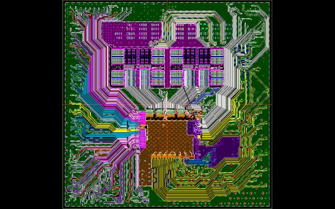
The Zen 2 design paradigm, compared to the first generation of Zen, has changed significantly. The new platform and core implementation is designed around small 8-core chiplets built on TSMC’s 7nm manufacturing process, and measure around 74-80 square millimeters. On these chiplets are two groups of four-cores arranged in a ‘core complex’, or CCX, which contains those four cores and a set of L3 cache – the L3 cache is doubled for Zen 2 over Zen 1.
Each full CPU, regardless of how many chiplets it has, is paired with a central IO die through Infinity Fabric links. The IO die acts as the central hub for all off-chip communications, as it houses all the PCIe lanes for the processor, as well as memory channels, and Infinity Fabric links to other chiplets or other CPUs. The IO die for the EPYC Rome processors is built on Global Foundries' 14nm process, however the consumer processor IO dies (which are smaller and contain fewer features) are built on the Global Foundries 12nm process.
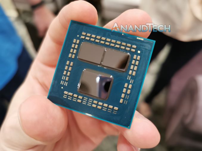
The consumer processors, known as ‘Matisse’ or Ryzen 3rd Gen or Ryzen 3000-series, will be offered with up to two chiplets for sixteen cores. AMD is launching six versions of Matisse on July 7th, from six cores to sixteen cores. The six and eight-core processors have one chiplet, while above this the parts will have two chiplets, but in all cases the IO die is the same. This means that every Zen 2 based Ryzen 3000 processor will have access to 24 PCIe 4.0 lanes and dual channel memory. Based on the announcements today, the prices will range from $199 for the Ryzen 5 3600, up to $700+ for the sixteen core (we’re waiting on final confirmation of this price).
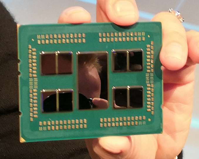
The EPYC Rome processors, built on these Zen 2 chiplets, will have up to eight of them, enabling a platform that can support up to 64 cores. As with the consumer processors, no chiplet can communicate directly with each other – each chiplet will only connect directly to the central IO die. That IO die houses links for eight memory channels, and up to 128 lanes of PCIe 4.0 connectivity.
AMD’s Roadmap
Before diving into the new product line, it is worth recapping where we currently sit in AMD’s planned roadmap.
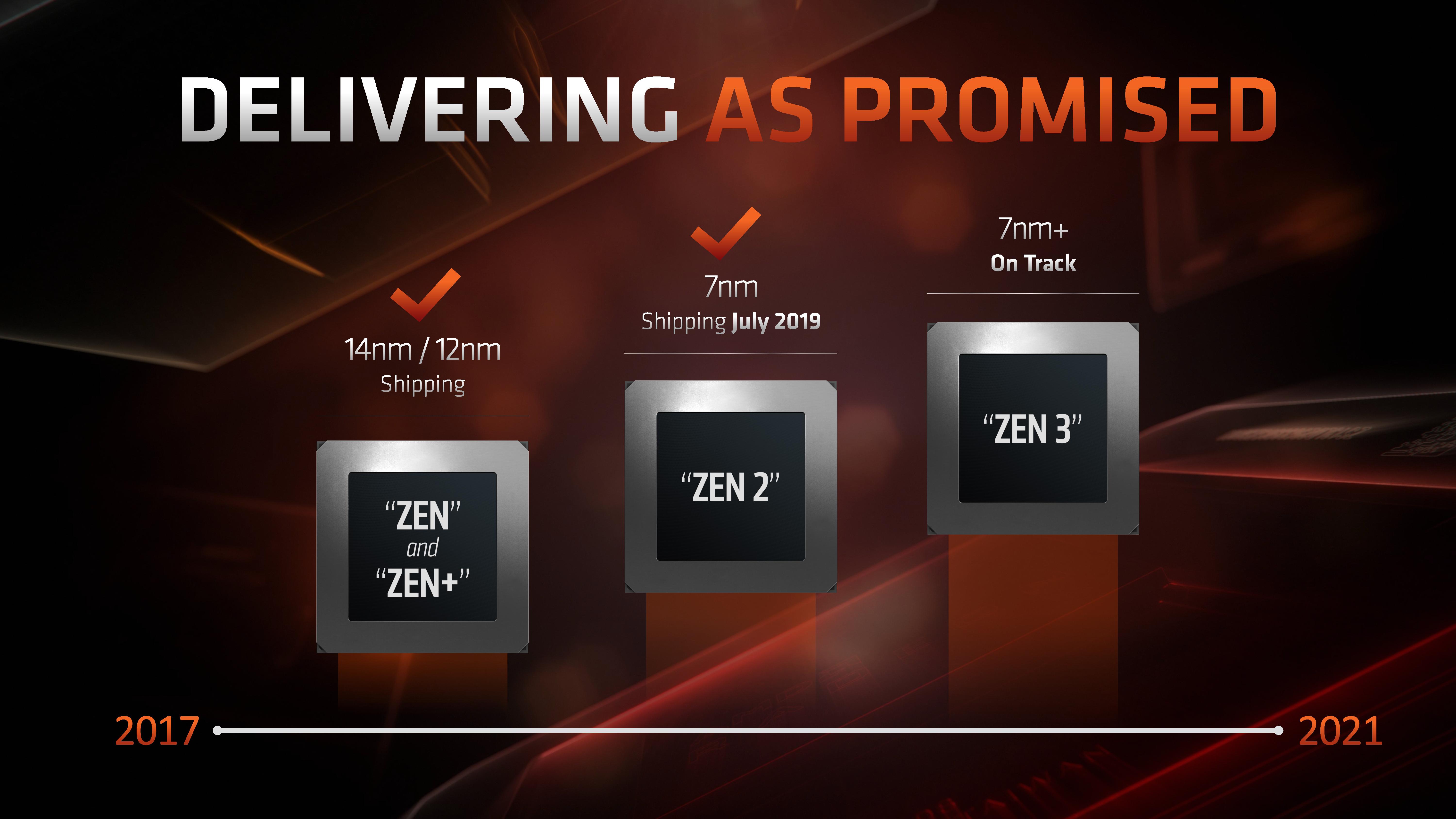
In previous roadmaps, showcasing AMD’s movement from Zen to Zen 2 and Zen 3, the company has explained that this multi-year structure will showcase Zen in 2017, Zen 2 in 2019, and Zen 3 by 2021. The cadence isn’t exactly a year, as it has depended on AMD’s design and manufacturing abilities, as well as agreements with its partners in the foundries and the current market forces.
AMD has stated that its plan for Zen 2 was to always launch on 7nm, which ended up being TSMC’s 7nm (Global Foundries wasn’t going to be ready in time for 7nm, and ultimately pulled the plug). The next generation Zen 3 is expected to align with an updated 7nm process, and at this point AMD has not made any comment about a potential ‘Zen 2+’ design in the works, although at this point we do not expect to see one.
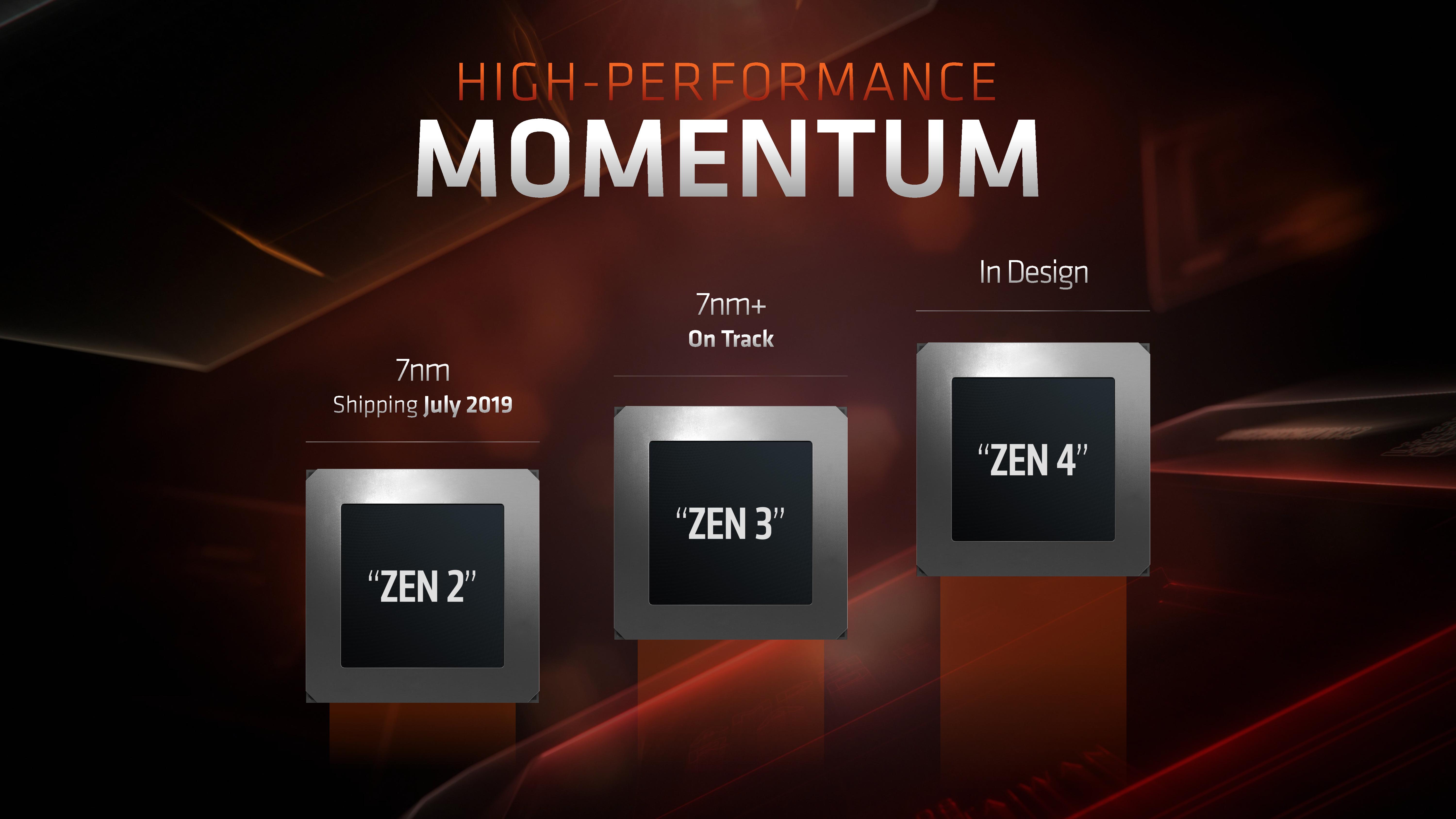
Beyond Zen 3, AMD has already stated that Zen 4 and Zen 5 are currently in various levels of their respective design stages, although the company has not committed to particular time frames or process node technologies. AMD has stated in the past that the paradigms of these platforms and processor designs are being set 3-5 years in advance, and the company states it has to make big bets every generation to ensure it can remain competitive.
For a small insight into Zen 4, in an interview with Forrest Norrod, SVP of AMD’s Enterprise, Embedded, and Semi-Custom group, at Computex, he exclusively revealed to AnandTech the code name of AMD’s Zen 4 EPYC processor: Genoa.
| AMD EPYC CPU Codenames | |||
| Gen | Year | Name | Cores |
| 1st | 2017 | Naples | 32 x Zen 1 |
| 2nd | 2019 | Rome | 64 x Zen 2 |
| 3rd | 2020 | Milan | ? x Zen 3 |
| 4th | ? | Genoa | ? x Zen 4 |
| 5th | ? | ? | ? x Zen 5 |
Forrest explained that the Zen 5 code name follows a similar pattern, but would not comment on the time frame for the Zen 4 product. Given that the Zen 3 design is expected mid-2020, that would put a Zen 4 product for late 2021/early 2022, if AMD follows its cadence. How this will play into AMD’s consumer roadmap plans is unclear at this point, and will depend on how AMD approaches its chiplet paradigm and any future adjustments to its packaging technology in order to enable further performance improvements.


216 Comments
View All Comments
nonoverclock - Wednesday, June 12, 2019 - link
It's related to platform power management.wurizen - Wednesday, June 12, 2019 - link
"Raw Memory Latency" graph shows 69ns for for 3200 and 3600 Mhz RAM. This "69ns" is irrelevant, right? Isn't the "high latency" associated with Ryzen and IF due to "Cross-CCX-Memory-Latency? This is suppose to be ~110ns at 3200 Mhz RAM as tested by PCPER/etc.... This in my experiences causes "micro-stuttering" in games like BO3/BF4/etc.... And, a "Ryzen-micro-stutter/pause" is different than a micro-stutter/pause associated with Intel. With Intel the micro-stutter/pause happens in BFV, for example, but they happen once or twice per match. With Ryzen, not only is the quality/feeling of the "micro-stutter/pause" different (seems worst), but it is constant throughout the match. One gets a feeling that it is not server-side, GPU side, nor WIndows 10 side. But, CPU-side issue... Infinity Fabric side. So, now Inifinity Fabric 2 is out. Is it 2.0 as in better? No more high latency? Is that 69ns Cross-CCX-memory latency? Why is AMD and Tech sites like Anand so... like... not talking about this?igavus - Wednesday, June 12, 2019 - link
You are misattributing things here. Your stutter is most def. not caused by memory access latency variations. For it to be visible on even an 144Hz monitor with the game running at the native rate, the differences would have to be obscenely high. That's just unrealistic.Not that it helps to determine what is causing your issues, but that's not it.
wurizen - Wednesday, June 12, 2019 - link
What?wurizen - Wednesday, June 12, 2019 - link
Maybe, you guys don't know what Cross-CCX-Memory-Latyency is... my main goal of commenting was what that SLIDE showing "Raw Memory Latency" refers to? Is it Inter-core-memory or Intra-core-memory (intra-core is the same as cross-ccx-memory)...inter-core memory is data being shuffled within the cores in a CCX module. Ryzen and Ryzen + had two CCX modules with 4 cores each, totaling 8 cores for the 2700x, as an example. If, the memory/data is traveling in the same CCX, the latency is fine and is even faster than Intel. This was true with Ryzen and Ryzen +.
The issue is when data and memory is being shuffled between the CCX modules, and when traversing the so called "Infinity Fabric." Intel uses a Ring Bus and doesn't have an equivalent measurement and data. Intel does have MESH with the x299 which is similar-ish to AMD's CCX and IF. But, Intel Mesh latency is lower (I think. But havent dug around since I dont care about it since I cant afford it)....
So... that is what Cross-CCX-memory-latency is... and that SLIDE shown on this article... WTF does that refer to? 69ns is similar to Intel Ring Bus memory latency, which have shown to be fast enough and is the standard in regards to latency that won't cause issues...
So... as PCPER tested, Ryzen Infinity Fanri 1.0 has a cross-ccx-latnecy to be around 110ns... and I stand my ground (its not bios/reinstallwindows/or windows scheduler/or user-error/or imperceptible/or a misunderstanding / or a mis-atribution (I think)) that it was the reason why I suffered "micro-pauses/stutters in some games. I had two systems at the time (3700k and R7-1700x) and so I was able to diagnose/observe/interpret what was happening....
Also.. I would like to add that the "Ryzen Micro-stutter-Pause" FEELS/LOOKS/BEHAVES different... weird, right?
deltaFx2 - Thursday, June 13, 2019 - link
You might "stand your ground" but that doesn't make it true. First of all, it's pretty clear you don't understand what you're talking about. Intel's Mesh is NOTHING like AMD's CCX. Intel Mesh is an alternative interconnect to ring bus; mesh scales better to many cores relative to ring. In theory mesh should be faster but for whatever reason intel's memory latency on skylake X parts are quite bad relative to skylake client (i.e. no bueno for gaming). I recall 70ns-ish for Skylake X vs 60ns for the Skylake client.Cross CCX memory latency should not matter unless you have shared memory across threads that span CCXs. Games don't need that many threads: 8 is overkill in many cases and each CCX can comfortably handle 8. Unless you pinned threads to cores and ran an experiment that conclusively showed that the issue was inter-ccx latency (I doubt it), your standing ground doesn't mean much. One could just as well argue that the microstutter was due to driver issues or other software/bios issues. Zen has been around for quite some time and if this was a widespread problem, we'd know.
wurizen - Friday, June 14, 2019 - link
Well, I did mention "similar-ish" of Mesh to Infinity Fabric. It's meshy. And, i guess, you get "comraderie" points for calling me out as "pretty clear you don't understand what you're talking about." That hurts, man! :("In theory... Mesh should be faster..." nice way to switch subjects, bruh. yeh, i can throw some at ya, bruh! what?
Cross-CCX-High-Memory-Latency DOES MATTER!
You know why? Because a game shuffles data randomly. It doesn't know that traversing said Data from Core 0 (residing in CCX 1) to Core 3 (in CCX 2) via Infinity Fabric means that there is a latency penalty.
Bruh
deltaFx2 - Friday, June 14, 2019 - link
Actually, no, you're wrong about the mesh. Intel has a logically unified L3 cache; i.e. any core can access any slice of the L3, or even one core can use the entire L3 for itself. AMD has a logically distributed L3 cache which means only the cores from the CCX can access its cache. You simply cannot have core 3 (CCX 0) fetch a line into CCX1's cache. The tradeoff is that the distributed L3 is much faster than the logically unified one but the logically unified one obviously offers better hit rates and does not suffer from sharing issues."Cross-CCX-High-Memory-Latency DOES MATTER!" Yes it does, no question about that. It matters when you have lock contention or shared memory that spans CCXs. In order to span CCXs, you should be using more than 8 threads (4 cores to a CCX, 2 threads per core). I don't think games are _that_ multithreaded. This article mentions a Windows 10 patch to ensure that threads get assigned to the same CCX before going to the adjacent one. It can be a problem for compute-intensive applications (y'know, real work), but games? I doubt it, and you should be able to fix it easily by pinning threads to cores in the same CCX.
deltaFx2 - Friday, June 14, 2019 - link
"shared memory that spans CCXs." -> shared DIRTY memory. i.e. core 8 writes data, core 0 wants to read. All other kinds of sharing are a non-issue. Each CCX gets a local copy of the data.wurizen - Friday, June 14, 2019 - link
Why do you keep on blabbing on about this? Are you trying to fix some sort of muscle?