Examining Intel's Ice Lake Processors: Taking a Bite of the Sunny Cove Microarchitecture
by Dr. Ian Cutress on July 30, 2019 9:30 AM EST- Posted in
- CPUs
- Intel
- 10nm
- Microarchitecture
- Ice Lake
- Project Athena
- Sunny Cove
- Gen11
Sunny Cove Microarchitecture: Going Deeper and Wider
Ice Lake falls under Intel’s ‘10th Gen Core’ family, and is based around the latest iteration of the ‘Core’ microarchitecture, which initially debuted over a decade ago and has received plenty of key critical enhancements and extra features along the way. Over the years we’ve seen improved prefetchers, smarter branch predictors, adjusted cache sizes and capabilities, deeper and wider execution, micro-op caches, accelerated calculation logic, and lower power operation, all designed to increase the instruction throughput, decrease cache misses, and improve power efficiency.
When Intel designs a new generation of Core, it tends to go in a lot of things: mobile CPUs, desktops, servers, sometimes embedded, new communications technologies, and plenty of other custom silicon besides. As a result, it has to scale, from low-end to high-end. One of Intel’s new Chief Architects, Jim Keller, says that Intel has a ‘milliwatt-to-megawatt’ strategy when it comes to product design, and it’s the Core microarchitecture that is currently bringing in the big $$$ to fund a lot of the R&D.
Before we go into the new Sunny Cove core, I should preface the explanations with a little warning. Intel’s previous microarchitecture update and design, Skylake, is Intel’s most profitable design ever. Part of that reason is that it has been around the block for four generations of products. Intel hasn’t changed the core in that time, for almost four years. At this point, we’ve been yearning for something that actually has changes. So please forgive a little excitement when covering a few of the more mundane updates.
Sunny Cove Front End
Despite the instruction entry point into the core being at the front-end. Intel didn’t say too much about Sunny Cove in this respect. Typically Intel keeps the details of its prefetchers and branch predictors secret, although CPU Architect Ronak Singhal did state that it is by-and-large similar to the Skylake design. Ronak has said that the branch predictor has increased accuracy, and that the average/effective load latency has decreased, and by and large the front-end of the CPU has been optimized for client (read consumers/end-users), rather than servers, which Skylake was. The internal structures of the branch predictor unit and prefetcher are larger according to Intel, which should help improve accuracy.
The L1 instruction cache is still a 32 KiB 8-way design, and there are still five decoders in play. These decoders are split as one complex decoder and four simple decoders, and they can supply up to five micro-ops per cycle. There’s nothing drastically new in terms of op fusion we are told, just the general expected improvements, plus additional support for the new AVX-512 instructions.

The micro-op cache gets an update here, from 1.5k entries to 2.25k entries. This is the first time that Intel has increased the micro-op cache size since Haswell, but it should be noted that the competition also has micro-op caches (ARM has 1.5k, AMD has 2k for Zen, 4k for Zen 2), and so refinement in this area is going to be critical. The micro-op cache can supply six micro-ops to the queue per cycle.
Overall, six micro-ops can be fed between the decoders/cache/direct micro-code per cycle. That is split between up to six per cycle from the cache, up to 5 from the decoders, and up to 4 from direct microcode (which gets fed through the complex decoder.
Out-of-Order Window
The micro-op queue, for rename/allocate/retire, has also increased. The design went from 182 micro-ops in Haswell to 224 in Skylake, but goes all the way up to 352 in Sunny Cove, a massive 57% increase. This will help managing which instructions are ready to be processed by the scheduler, although this often comes at the penalty of power. This is one of the advantages of using a smaller process node – there’s more power budget to go around, allowing a CPU team to design bigger queues.
| AnandTech | Haswell | Skylake | Sunny Cove |
| Reorder Buffer | 182 | 224 | 352 |
| In-Flight Stores | 72 | 72 | 128 |
| In-Flight Loads | 42 | 56 | 72 |
With the increased queue size, Intel also reports that support for in-flight loads and stores has increased: up from 72 loads in Skylake to 128 in Sunny Cove, and up from 56 stores in Skylake to 72 in Sunny Cove. This means that the in-flight load/store ratio is more weighted in favor of loads, which Intel states is part of the more user-focused design where loads end up being more important than stores.
Back End
This is where the fun happens. As with previous Intel designs over the years, we still have a unified scheduler for both integer and vector operations, however they are split between four different reservation stations depending on what operation is needed:
- One for four ALU ports, accepts 4 micro-ops/cycle
- One for two Store ports, accepts 2 micro-ops/cycle
- One for a pair of AGUs, one load, one store, accepts 2 micro-ops/cycle
- One for a pair of AGUs, one load, one store, accepts 2 micro-ops/cycle
In total, the number of execution ports has increased from 8 in Skylake to 10 in Sunny Cove. This allows for 10 micro-ops per cycle to be dispatched from the reorder buffer, a 25% increase. The two new ports lie in different areas: Skylake had 3 AGUs, supporting two loads and one store per cycle, but Sunny Cove now has 4 AGUs, for two loads and two stores per cycle. The other new port is a store data port. With these changes, the L1 data cache can now support two stores per cycle, effectively doubling the L1 store bandwidth.
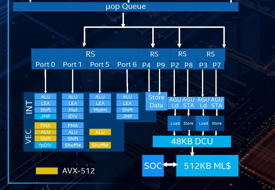
The L1 Data cache has increased, for the first time in over a decade. Intel has moved from a 32 KiB 8-way design up to a 48 KiB 12-way design, which should help reduce data cache misses significantly. This combined with the micro-op cache size increase is one of the easiest ways to reduce cache miss penalties. (For comparison, in Zen 2 AMD halved its L1-I size and doubled its micro-op cache, which it felt was a more efficient way of improving instruction throughput, but also the silicon area design had to be managed.)
Intel has also increased the L2 cache, up from 256 KiB to 512 KiB, and it is still non-inclusive of the L1 with a write-back policy. In order to assist the L2, the L2 TLB page table arrangement has also been improved, with up to 2k entries at 4K, 1k entries for 2M/4M (new, used to be shared with 4K), and up from 16 entries to 1024 entries at 1G. The cache improvements on Sunny Cove are certainly expected to work in Intel’s favor, especially when it comes to the enhanced graphics part of the design.
On a core-to-core level, Intel's recent designs have the following configurations:
| Microarchitecture Comparison | ||||||
| Skylake | Cannon Lake | Sunny Cove* | Zen | Zen 2 | ||
| L1-D Cache |
32 KiB/core 8-way |
32 KiB/core 8-way |
48 KiB/core 12-way |
32 KiB/core 8-way |
32 KiB/core 8-way |
|
| L1-I Cache |
32 KiB/core 8-way |
32 KiB/core 8-way |
32 KiB/core 8-way |
64 KiB/core 4-way |
32 KiB/core 8-way |
|
| L2 Cache |
256 KiB/core 4-way |
256 KiB/core 4-way |
512 KiB/core 8-way |
512 KiB/core 8-way |
512 KiB/core 8-way |
|
| L3 Cache |
2 MiB/core 16-way |
2 MiB/core 16-way |
2 MiB/core 16-way |
2 MiB/core | 4 MiB/core | |
| L3 Cache Type | Inclusive | Inclusive | Inclusive | Non-Inclusive | Non-Inclusive | |
| Decode | 4 + 1 | 4 + 1 | 4 + 1 | 4 | 4 | |
| uOP Cache | 1.5k | 1.5k | 2.25k | 2k | 4k | |
| Reorder Buffer | 224 | 224 | 352 | 192 | 224 | |
| Execution Ports | 8 | 8 | 10 | 10 | 11 | |
| AGUs | 2 + 1 | 2 + 1 | 2 + 2 | 1 + 1 | 2 + 1 | |
| AVX-512 | - | 1 x FMA | 1 x FMA | - | ||
| * Sunny Cove numbers for Client. Server will have different L2/L3 cache and FMA, like Skylake | ||||||
For the execution ports, now that Intel has moved AVX-512 into the mainstream Core design, there are a few changes. AVX-512 is now supported on Port 0 (FMA, ALU, Shift) and Port 5 (ALU, Shuffle). There is only one AVX-512 port, but also a 256-bit FMA port, so either 1x512-bit or 2x256-bit throughput is possible.
Overall the design allows for:
| Back-End Execution Resources | ||||||||
| Skylake | Port | Sunny Cove | ||||||
| Integer | ||||||||
| JMP | Shift | ALU | 0 | ALU | LEA | Shift | JMP | |
| LEA | ALU | 1 | ALU | LEA | Mul | iDIV | ||
| Mul | LEA | ALU | 5 | ALU | LEA | MulHi | ||
| JMP | Shift | ALU | 6 | ALU | LEA | Shift | JMP | |
| Vector / FP | ||||||||
| fpDIV | Shift | ALU | FMA | 0 | FMA | ALU | Shift | fpDIV |
| Shift | ALU | FMA | 1 | FMA | ALU | Shift | Shuffle | |
| Shuffle | ALU | FMA | 5 | FMA | ALU | Shuffle | ||
The parts highlighted in bold are different in the Sunny Cove core.
The TL;DR
The core improvements can be summed up as follows:
- Better prefetchers and branch predictors
- +50% L1 Data Cache
- +100% L1 Store Bandwidth
- +100% L2 Cache w/improved L2 TLB
- +50% Micro-op Cache
- +25% uops/cycle into reorder buffer
- +57% reorder buffer size
- +25% execution ports
- AVX-512 with VNNI
Add in better memory support (Up to LPDDR4X-3733) and better graphics (64 EUs of Gen11), and it’s a really nice update.
For all of this, Intel is promoting a +18% IPC increase over Skylake, which ranges from 0.98x to 1.40x depending on the workload (SPEC2006, SPEC2017, SYSMark 2014SE, WebXPRT, CineBench), or a +47% increase in real world tasks against Broadwell.

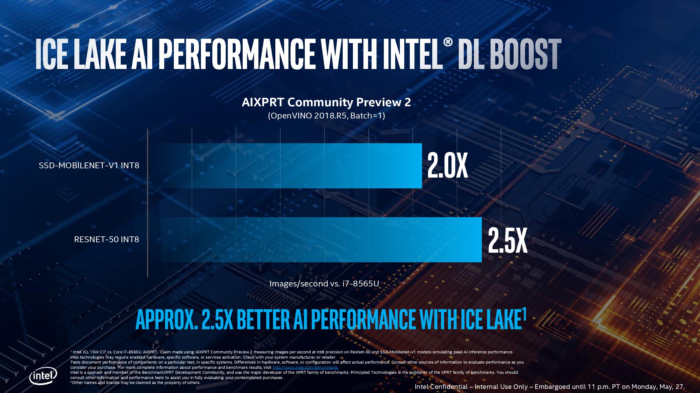
When AVX512 is in play, with DLBoost, Intel is promoting a 2.0x-2.5x increase against the best Whiskey Lake has to offer.
We’ll cover Intel’s claims later in the analysis.


107 Comments
View All Comments
repoman27 - Tuesday, July 30, 2019 - link
"It stands to reason then that the smaller package is for lower performance and low power options, despite being exactly the same silicon."I know the die floorplans are the same, but have Intel ever actually confirmed that U and Y (or H and S series for that matter) are the exact same silicon? Is it strictly binning and packaging that separates the platforms, or is there a slight tweak to the manufacturing process to target lower power / higher frequencies? Intel production roadmaps would seem to indicate this isn't just a binning situation, but I've never been entirely certain on that point.
And isn't Comet Lake-U 6+2 more likely to be 25 W, with Whiskey Lake-U 4+2 continuing to pull 15 W duty alongside Ice Lake-U 4+2?
CaedenV - Tuesday, July 30, 2019 - link
Those goals for Aethena are OK, but my old Dell XPS 12 with a carousel frame hit all of those except biometric, and wake from sleep in <1 sec... well, and the bezel... but that was due to the carousel design which I would LOVE to come back in a more modern form.Not saying these goals are bad... but if a 6 year old midrange laptop can hit almost all of them, then this isn't exactly aiming for something amazing.
AshlayW - Tuesday, July 30, 2019 - link
Quad core for 179 USD? What is this, 2015? No thanks.HStewart - Tuesday, July 30, 2019 - link
You do realize these are ultra-portable low power cpu's and not desktop chipsSamus - Tuesday, July 30, 2019 - link
Intel is a mess right now, the execution of this along with the naming scheme is ridiculous.shabby - Tuesday, July 30, 2019 - link
18% ipc gain and 20% clock lossPlace your bets how intel will spin this.
CHADBOGA - Tuesday, July 30, 2019 - link
I'm quite disappointed the issue of security mitigation in hardware was not addressed. o_OCityBlue - Saturday, August 3, 2019 - link
Disappointed, but not surprised.Security (and by inference the performance overhead required to implement proper security) is not important according to Anandtech/Ian Cutress. Which is obvious nonsense, so the only logical conclusion is that Anandtech are now a thoroughly biased outfit incapable of any critical reporting, which is quite sad particularly as it means all their articles (particularly when they relate to Intel) have to be read with a very heavy dose of cynicism.
eek2121 - Wednesday, July 31, 2019 - link
That picture of you biting a wafer is priceless.Santoval - Wednesday, July 31, 2019 - link
If Ice Lake-U has a ~3.5% higher single core performance (and, assuming the "multi-core overhead" is the same, multi-core performance as well) than Whiskey Lake-U despite having a 20% lower single core boost clock, then Sunny Cove must be an extremely impressive μarch. Or, er, that might not actually be the case : Ice Lake-U has a 18% higher IPC than the *original* Skylake of 2015, not Whiskey Lake. While Whiskey Lake is basically the same design it must have a somewhat higher IPC due to its much more mature process node and other optimizations.Let's be conservative and assume that Ice Lake-U (more specifically Sunny Cove) has a nice round 15% higher IPC than Whiskey Lake-U, with both at 15W. In that case, at a 20% lower boost clock Ice Lake-U should have a 5% lower performance than Whiskey Lake-U. Where is that +3.5% performance derived from then?
Even if we assumed that Ice Lake-U 18% IPC edge is over Whiskey Lake-U (highly unlikely, otherwise Intel would not have dug out the original Skylake from its computing grave) that would still translate to Ice Lake-U having a 1.5% lower single core performance than Whiskey Lake-U, rather than being 3.5% faster than it.
Maybe, just maybe, this is why Intel used just a single synthetic benchmark (surely compiled with aggressive flags and optimized for Intel CPUs) for that graph and avoided to disclose other synthetic benchmarks and real world use benchmarks? Is this also why they avoided to talk about CPU performance of Ice Lake in their Computex presentation, and instead focused on iGPU, Wifi and AI performance?
Based on the disclosed clocks and the "disclosed" (in obfuscated form) IPC of Ice Lake-U I just cannot see it being in any way faster than Whiskey Lake-U. It will probably also have worse power efficiency, since it has the same or higher TDP range at a much lower clock.