Examining Intel's Ice Lake Processors: Taking a Bite of the Sunny Cove Microarchitecture
by Dr. Ian Cutress on July 30, 2019 9:30 AM EST- Posted in
- CPUs
- Intel
- 10nm
- Microarchitecture
- Ice Lake
- Project Athena
- Sunny Cove
- Gen11
Intel’s Ice Lake and Sunny Cove
A Welcome Update, with Questions on Execution
When launching a new mobile product using a new processor design, all the parts have to come together to make it work. This means all of the following:
- The microarchitecture design
- SoC implementation
- Manufacturing
- Co-operation with partners/OEMs
- Time to Market
- Messaging
- Marketing
- Interactions with the press and consumers
- Promotion
- Price
- Competitiveness
Any one of these segments could make or break the next wave of innovation (a key phrase Intel likes to use). With Intel’s 10nm manufacturing process, and the 10th Gen Core 'Ice Lake' design, we’re moving along each of these points in turn, and it is interesting to see what the final reflection will be several years down the line. From our perspective, we now have extensive details on the core and the SoC, and Intel is slowly moving into product phase by the end of the year. We can evaluate what we’ve seen.
The Core and the SoC
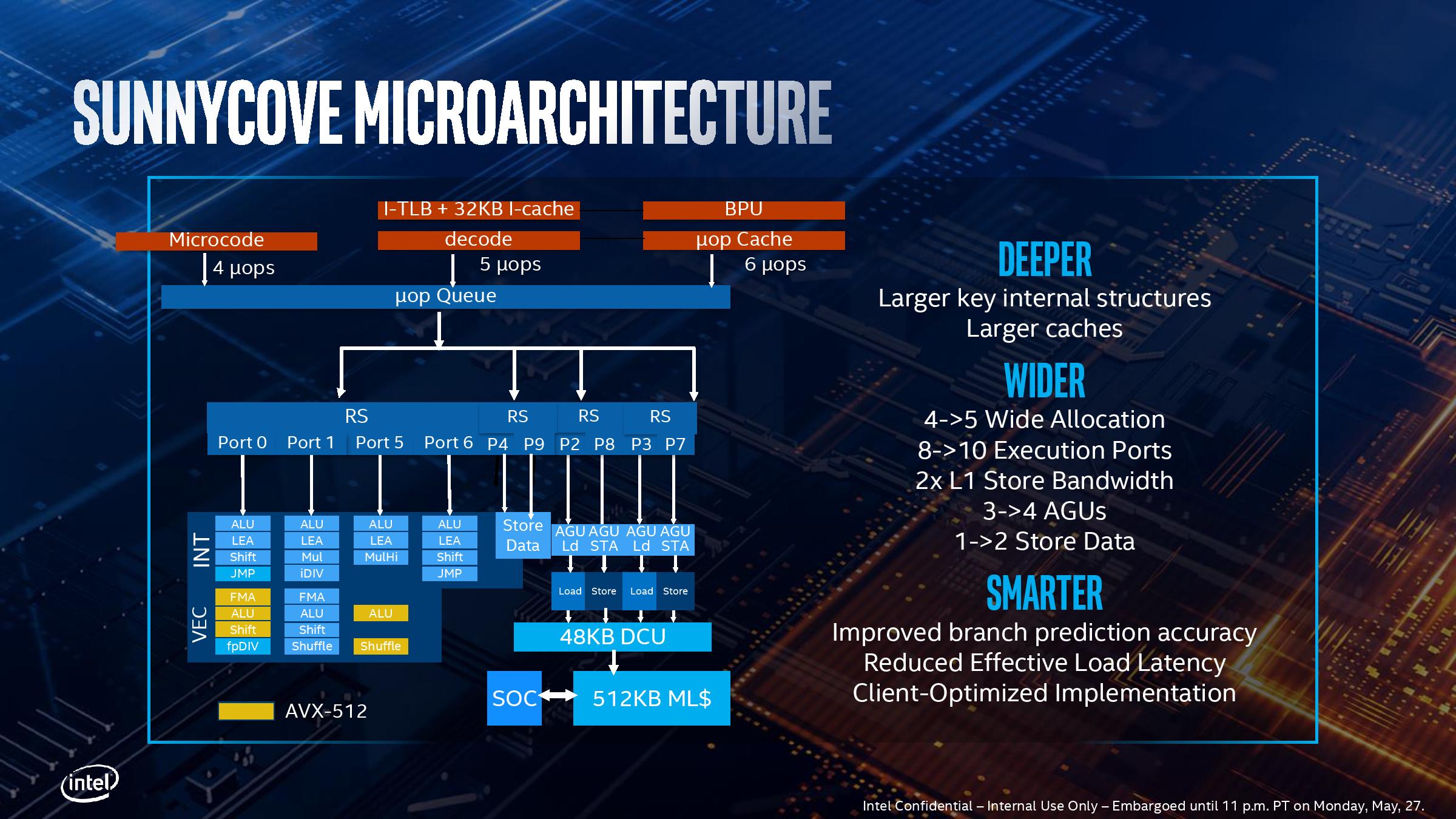
Having ‘not another Skylake’ is a huge sigh of relief. With every new microarchitecture update, especially significant ones, we like to see how the power budget is being used and what key structures within the microarchitecture have been improved and expanded upon. The team behind the Sunny Cove core have listed some impressive hard numbers, with doubling the L1 store bandwidth, making significant L1 and L2 cache adjustments, increasing the reorder buffer a whopping +57%, and moving to a 10-port execution unit design. The inclusion of AVX-512 is welcomed by parts of the community for sure, although I expect not as many as Intel would like (this leads onto Intel’s DLBoost strategy, I’ll mention later). Assuming we can get the same +18% IPC metrics that Intel does, this is a great uplift and it will be exciting to see where we go from here.
On the SoC, the big improvements to the graphics and the memory controller are my important ones here. Intel is taking integrated graphics seriously again, with an improved 64 EU design that promises to match AMD’s best at 25W. Intel has improved its memory controller significantly here, now supporting LPDDR4-3733 and DDR4-3200, which helps given that the graphics hardware is always craving memory bandwidth.
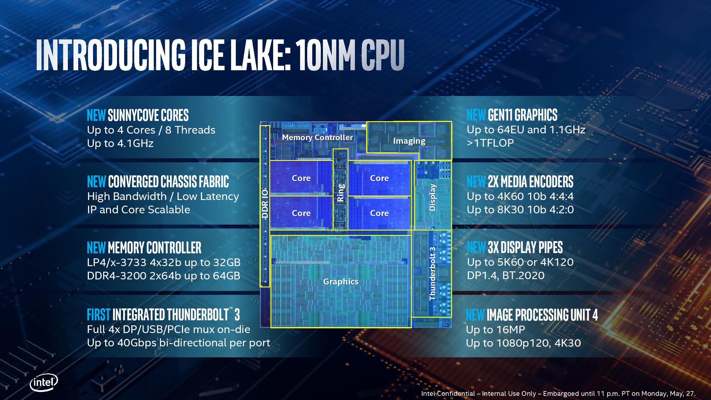
Adding Thunderbolt 3 to the SoC is going to help drive adoption in the mobile space, however speaking to a number of press, we think that because TB3 still requires an expensive controller on the device end, that the standard still has that high-cost to entry barrier, even if it ends up being cheaper for host implementation. Until non-Intel TB3 device controllers hit the market, the biggest benefit here is going to be potential support for the USB4 standard. With respect to the Wi-Fi 6 enablement, I’m not so enthused here, as it still requires an additional Intel-only proprietary CNVi module, forcing OEMs to go down an Intel route. If Intel made the CNVi standard open to all, I’d be making a bigger deal about this.
Manufacturing and Time To Market
The fact that Intel is going to end up competing against itself, with Ice Lake-U against Comet Lake-U, is akin to shooting yourself in the foot. Ultimately we expect Ice Lake-U to be focused on the premium market through Intel’s Project Athena, but Comet Lake-U is likely to span from budget to premium as well, especially if it ends up supporting more cores than Ice Lake. Ice Lake should have been a 2017 product, and Intel is only now at a point where it believes its 10nm products are viable for the market, which leads to questions on if the process is even profitable, and how many chips are going to be made available to OEMs – again, because of Project Athena, only key OEM customers going for those premium devices are going to launch initially, tailoring the messaging towards that premium feel.
Questions still surround Intel’s 10nm viability, especially given that the company has promised it is going to be producing high core count Xeons on this process node. Hopefully we can get an update on that.
Ice Lake Messaging, and Project Athena
As mentioned, the whole deal with Whiskey Lake and Comet Lake single thread CPU performance being similar to Ice Lake is going to be a mess. Part of this is down to the messaging for sure, whereby both Ice Lake and Comet Lake are going to be Intel 10th Gen, with Core i7 and Core i5/i3 variants. The only way to distinguish between the two is that Ice Lake has a G in the SKU and Comet Lake has a U, details that some of Intel’s own partners don’t disclose on product pages on websites.
One thing that Intel could lean on is the AVX-512 in Ice Lake, and its DL Boost strategy. Despite AVX-512 being inside Intel’s Xeons, the amount of ‘consumer-grade’ software that uses it is very minimal. By moving it into the consumer platforms, and enabling features like VNNI, Intel wants to drive AI-software solutions into the market. One example we were given was the ability for image software to sort images by what it detects in them – and having this all done locally (and securely) on the CPU, rather than the cloud. If Intel can execute on DL Boost for consumers, it could be a big win, and an easy benefit over the competition.
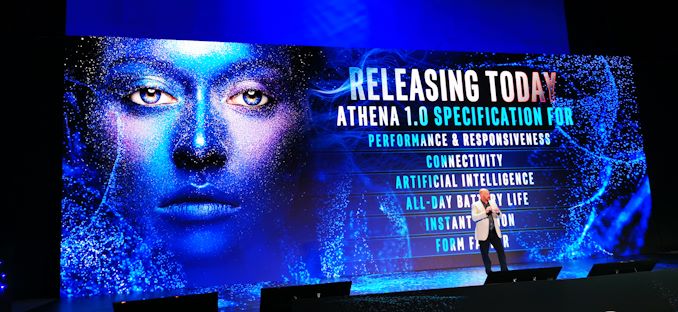
Turning to Project Athena – I’m all in favor of driving innovation forward and defining specifications that help push new and innovative form factors to enhance the user experience. But as you might have guessed, as it stands, I’m not its biggest fan. The Athena ecosystem is its own closed playground – in order for OEMs to play ball, they have to meet a number of requirements, a sizable chunk of which are only beneficial through Intel-only hardware. For example, Athena devices need Wi-Fi 6, which can be provided by an M.2 module or a CNVi RF chip. Athena devices also need substantial battery life, and the best way to achieve that is by using a CNVi RF option – but Intel is the only one that can make them because the CNVi standard is proprietary.
If an OEM doesn’t want to use Intel’s Wi-Fi 6 solution, then it makes it harder to develop an Athena certified device. It means that OEMs have to play Intel’s game in order to compete in the space. For me, that’s a high entry fee. Sure, the certified devices at the end of day are likely to be great, but if they all have Intel Wi-Fi 6, then where’s the variation? Perhaps I’m a little altruistic here: Intel is trying to create its own certification program and to play by the rules might require investing in Intel-only designed controllers. But I feel that an effort like this works best when there’s competition at every level.
Competition
On a core-to-core level, Intel's recent designs have the following configurations:
| Microarchitecture Comparison | ||||||
| Skylake | Cannon Lake | Sunny Cove* | Zen | Zen 2 | ||
| L1-D Cache |
32 KiB/core 8-way |
32 KiB/core 8-way |
48 KiB/core 12-way |
32 KiB/core 8-way |
32 KiB/core 8-way |
|
| L1-I Cache |
32 KiB/core 8-way |
32 KiB/core 8-way |
32 KiB/core 8-way |
64 KiB/core 4-way |
32 KiB/core 8-way |
|
| L2 Cache |
256 KiB/core 4-way |
256 KiB/core 4-way |
512 KiB/core 8-way |
512 KiB/core 8-way |
512 KiB/core 8-way |
|
| L3 Cache |
2 MiB/core 16-way |
2 MiB/core 16-way |
2 MiB/core 16-way |
2 MiB/core | 4 MiB/core | |
| L3 Cache Type | Inclusive | Inclusive | Inclusive | Non-Inclusive | Non-Inclusive | |
| Decode | 4 + 1 | 4 + 1 | 4 + 1 | 4 | 4 | |
| uOP Cache | 1.5k | 1.5k | 2.25k | 2k | 4k | |
| Reorder Buffer | 224 | 224 | 352 | 192 | 224 | |
| Execution Ports | 8 | 8 | 10 | 10 | 11 | |
| AGUs | 2 + 1 | 2 + 1 | 2 + 2 | 1 + 1 | 2 + 1 | |
| AVX-512 | - | 1 x FMA | 1 x FMA | - | ||
| * Sunny Cove numbers for Client. Server will have different L2/L3 cache and FMA, like Skylake | ||||||
Where AMD has reduced the size of the L1-D cache (to fit in a 4k micro-op cache), Intel has increased it. Both AMD and Intel now sit with 512 KiB L2 caches, although AMD is 4 MiB of non-inclusive cache to Intel's 2 MiB of inclusive cache. Intel has a much larger re-order buffer, and made improvements to its address generation units to help feed the cores. It's becoming ever more important to feed the beast.
Final Thought of the Day
Looking through the Ice Lake and Sunny Cove design, I have to give kudos to Intel’s engineers. The core microarchitecture looks solid, and there is no doubt that Intel will have a raw single thread performance advantage in the mobile space. I’m glad that Intel is taking its graphics solutions seriously again, and between the CPU and GPU, it’s good to see that extra power budget going to good use. I can’t wait to have the hardware on hand.
If you’re listening Intel, please consider the following: I haven’t seen any plans to bring Ice Lake to the desktop, but can we get a quad-core Ice Lake-U at 35W in a desktop processor form factor, for $179?


107 Comments
View All Comments
Billy Tallis - Wednesday, July 31, 2019 - link
A lot of the chemicals used in wafer processing are quite nasty. A bare wafer itself is pretty harmless unless you grind it up and inhale it. Solid elemental silicon or silicon dioxide is safe to handle.repoman27 - Tuesday, July 30, 2019 - link
I understand that there are embargos which must be respected and that Anandtech does not like to trade in unsubstantiated rumors, but much of what is presented regarding packaging and power seems a bit wishy-washy.Wikichip has had photos of both sides of the Ice Lake U and Y packages posted for some time now. Furthermore, Intel's product briefs are very clear on the power for each series:
Ice Lake Y: Nominal TDP 9 W, cTDP Down 8 W on Core i3 only, cTDP Up 12 W but N/A on Core i3,
Ice Lake U: Nominal TDP 15 W, cTDP Down 12 W (13 W for some UHD parts), cTDP Up 25 W
AFAIK, no 28 W Ice Lake-U parts have been announced by Intel yet, but they most likely are in the works.
And you can cite whatever reasons you care to, but by all reports Intel was initially targeting a 5.2 W TDP for Ice Lake-Y 4+2, and that entire platform has been solidly shifted into the 8-12 W range.
Also, it should be noted that the 14nm 300 Series chipsets that Intel has been shipping for some time now are all Cannon Point, which was originally designed to complement Cannon Lake, and are almost identical in terms of capabilities to the 400 Series. And the particular designation for the Ice Lake PCH-LP according to Intel is "495 Series".
James5mith - Tuesday, July 30, 2019 - link
Ian,You either have your graph or your paragraph about the store/load performance increases reversed.
Graph says 72 -> 128 stores, 56 -> 72 loads. The paragraph below it says 72-128 loads, 56-> 72 stores.
ksec - Tuesday, July 30, 2019 - link
While I do enjoy and mostly want to read Dr Ian Cutress article, I seriously don't want to read Intel's marketing hype. Action and Results speaks louder than Powerpoint slides. Ship it, let Anandtech test it. And we make an opinion on it.Targon - Tuesday, July 30, 2019 - link
The Ryzen 7 3700U is a Zen+ part on 12nm, without the big IPC plus clock speed improvements seen with the desktop CPUs. As a result, Intel is doing a comparison against the previous generation products for laptops.In laptops, getting max turbo or boost for more than one second is rare. Yea, Intel can put a laptop chip on a board on a bench without any enclosure to show the chip, but real world speeds will be quite a bit lower. That is true for both AMD as well as Intel, and it is up to the OEMs to come up with a design to keep the chips cool enough to run faster than the competition.
AMD knows what is going on, so if I am correct, AMD will move up the release of the next generation of laptop chips to November. If AMD does the right thing, AMD will call the new chips the 3250U, 3400U, 3600U, and 3800U to bring consistency with desktop naming conventions. These new chips would be 7nm with either Vega or Navi, for an APU it is less important than going 7nm for both.
Drumsticks - Tuesday, July 30, 2019 - link
Keep in mind, the only comparison they did with Ryzen (I think) was Graphics, not CPU. I'd imagine the Icelake chips have a solid CPU lead against quad core Ryzen based on Zen/Zen+. Zen 2 will certainly help close that gap, but it should still be roughly 15-20% behind Icelake in IPC, and I certainly won't be ahead that much on frequency.Fulljack - Wednesday, July 31, 2019 - link
I think in Q4 19 they'd release Ryzen 4000 series (based on Zen 2) and call it day, like last year or two year ago.they'll be 4300U, 4500U, and 4700U for U-series and 4350H, 4550H, and 4750H for high-performance part with integrated graphics based on Navi.
but since Zen 2 has 8 cores now on each CCX, they'd probably also sell 6-core and 8-core part, but I don't know if they'll release it on U-series, though.
Apple Worshipper - Tuesday, July 30, 2019 - link
Thanks Ian ! So how does Ice Lake purportedly stand next to Apple’s A12x in iPad Pro based on the Spec scores ?PeachNCream - Tuesday, July 30, 2019 - link
More importantly, how does Ice Lake taste?HStewart - Tuesday, July 30, 2019 - link
I have seen anything that was successfully comparing x86 based cpus with AEM based cpusBut one things - that makes all this MacBook ARM stuff meaningless to me is one sheer fact - Apple has yet to release development tools for iOS on actual iOS. It might be Apple trying force Macs for development but Apples own development tools don't run on iOS