Examining Intel's Ice Lake Processors: Taking a Bite of the Sunny Cove Microarchitecture
by Dr. Ian Cutress on July 30, 2019 9:30 AM EST- Posted in
- CPUs
- Intel
- 10nm
- Microarchitecture
- Ice Lake
- Project Athena
- Sunny Cove
- Gen11
Gen11 Graphics: Competing for 1080p Gaming
The new message from Intel is that it is driving to deliver deep gaming experiences with its technology, and the nod to the future is specifically what it wants to do with its graphics technology. Until the company is ready with its Xe designs for 2020 and beyond, it wants to start to lead the way with better integrated designs. That starts with Ice Lake, where the most powerful version of Ice Lake will offer over 1TF of compute performance, support higher resolution HEVC, better display pipes, an enhanced rasterizer, and support for Adaptive Sync.
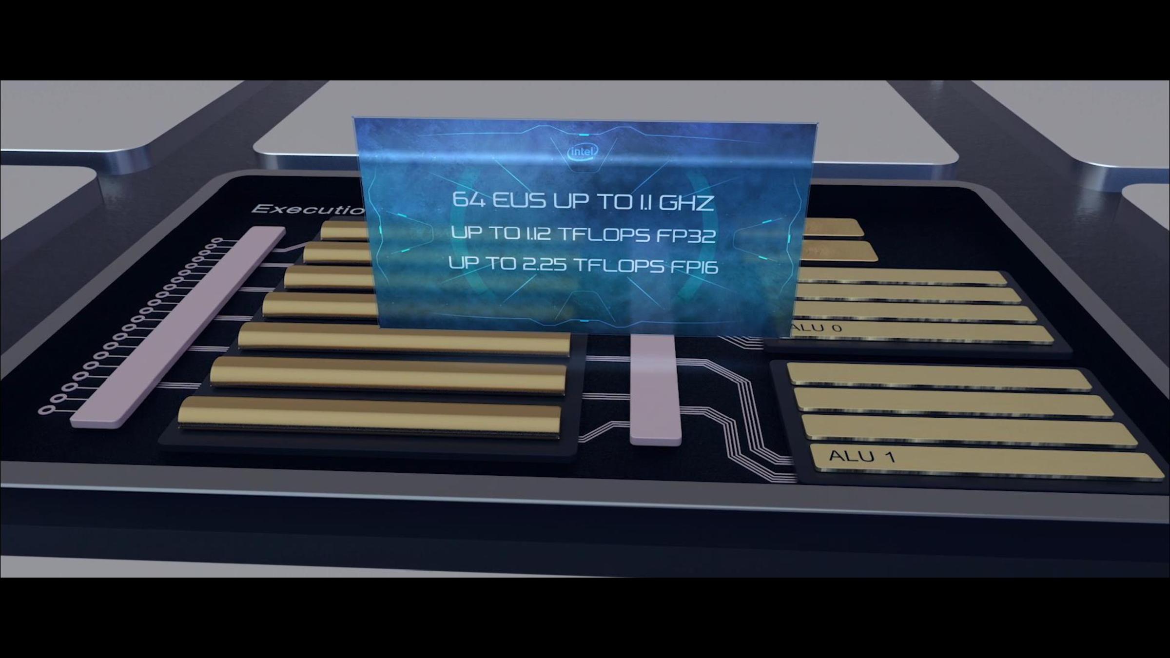
The key words in that last sentence were ‘the most powerful version’. Because Intel hasn’t really spoken about its product stack yet, the company has been leading with its most powerful Iris Plus designs. We assume this means 28W? That means its high-end performance products, in the best designs, with the fastest memory. Compared to the standard Gen9 implementation of 24 execution units at 1150 MHz turbo, the best Ice Lake Gen11 design will deliver 64 execution units up to a 1100 MHz frequency, good for 1.15 TF of FP32 performance, or 2.30 TF of FP16 performance. Intel promise up to 1.8x better frame rates in games with the best Ice Lake compared to an average 8th Gen Core (Kaby Lake) Gen9 implementation. Intel doesn’t compare the results to a hypothetical Cannon Lake Gen10 implementation.
Intel hasn’t stated how many graphics configurations it will offer, but there would appear to be several given what information has leaked out already. The high-end design with 64 execution units will be called Iris Plus, but there will be a ‘UHD’ version for mid-range and low-end parts, however Intel has not stated how many execution units these parts will have. We suspect that standard dividers will be in play, with 24/32/48 EU designs possible as different parts of the GPU are fused off. There may be some potential for increased frequency in these designs, reducing latency, but ultimately reduced performance over the top design.
It should be noted that Intel is promoting the top model as being suitable for 1080p low-to-mid gaming, which would imply that models with fewer execution units may struggle to hit those highs with different EU counts. Until Intel gives us a full and proper product list, it is hard to tell at this point.
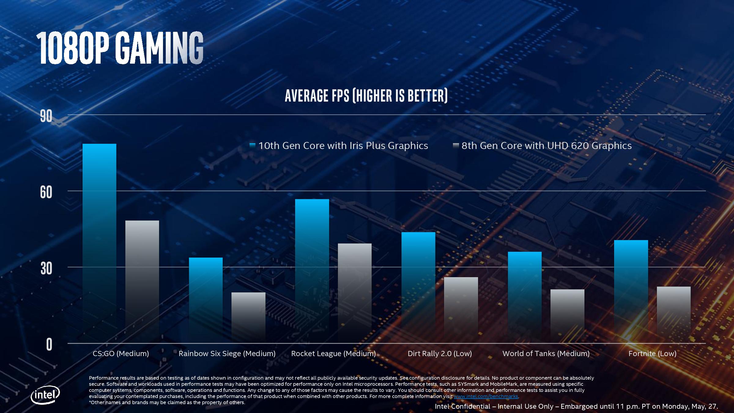
This slide, for example, shows where Intel expects its highest Ice Lake implementation to perform compared to the standard 8th Gen solution. As part of Computex, Intel also showed off some different data:
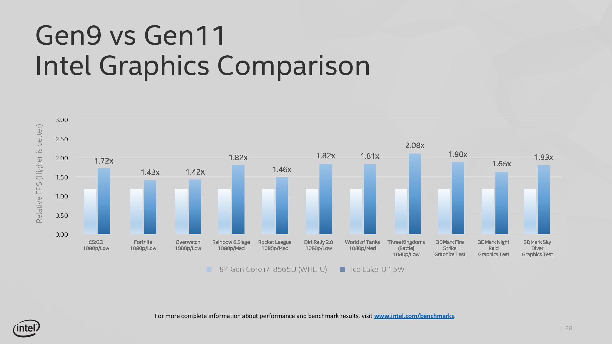
This graph shows relative FPS, rather than actual FPS, so it’s hard to see if certain games are just hitting 30 FPS in the highest mode. The results here are a function of the combination of increased EU count but also memory bandwidth.
Features for All
There are a number of features that all of the Gen11 graphics implementations will get, regardless of its number of execution units.
For its fixed function units, Gen11 supports two HEVC 10-bit encode pipelines, either two 4K60 4:4:4 streams simultaneously or one 8K30 4:2:2 stream using both pipelines at once. On display pipes, Gen11 has access to three 4K pipes split between DP1.4 HBR3 and HDMI 2.0b. There is also support for 2x 5K60 or 1x 4K120 with a 10-bit color depth.
The rasterizer gets an upgrade, and will now do 16 pixels per clock or 32 bilinear filtered texels per clock. Intel also gives some insight into the cache arrangements, with the execution units having their own 3 MiB of L3 cache and 0.5 MiB of shared local memory.
Intel recommends that to get the best out of the graphics, it should be paired with LPDDR4X-3733 memory in order to extract a healthy 50-60 GB/s bandwidth, and we should expect a number of Project Athena approved designs do just that. However, at the lower end of Ice Lake devices, we might see single channel DDR4 designs take over due to costs, which might limit performance. As always for integrated graphics, memory bandwidth is often a major bottleneck in performance. Back when Intel had eDRAM enabled Crystalwell designs, those chips were good for 50 GB/s bidirectional bandwidth, and we are almost at that stage with DRAM bandwidth designs now. It should be noted that there are tradeoffs with memory support: LPDDR4/X supports 4x 32b channels up to 32 GB with super low power consumption modes, but if users want more capacity, they’ll have to look to DDR4-3200 with 2x 64b channels up to 64 GB, but lose some performance and power savings.
Variable Rate Shading
A feature being implemented in Gen11 is Variable Rate Shading. VRS is a game-dependent technology that allows the GPU adjust the shading performance of the scene render based on what areas are important. All games currently do shading on a per-pixel basis, meaning that each pixel has a full calculation and that data is transferred to the final image. With VRS, shading is calculated over several pixels at once – essentially doing pixel shading in a coarser, lower-resolution manner – to save post-processing time by using averaged data.
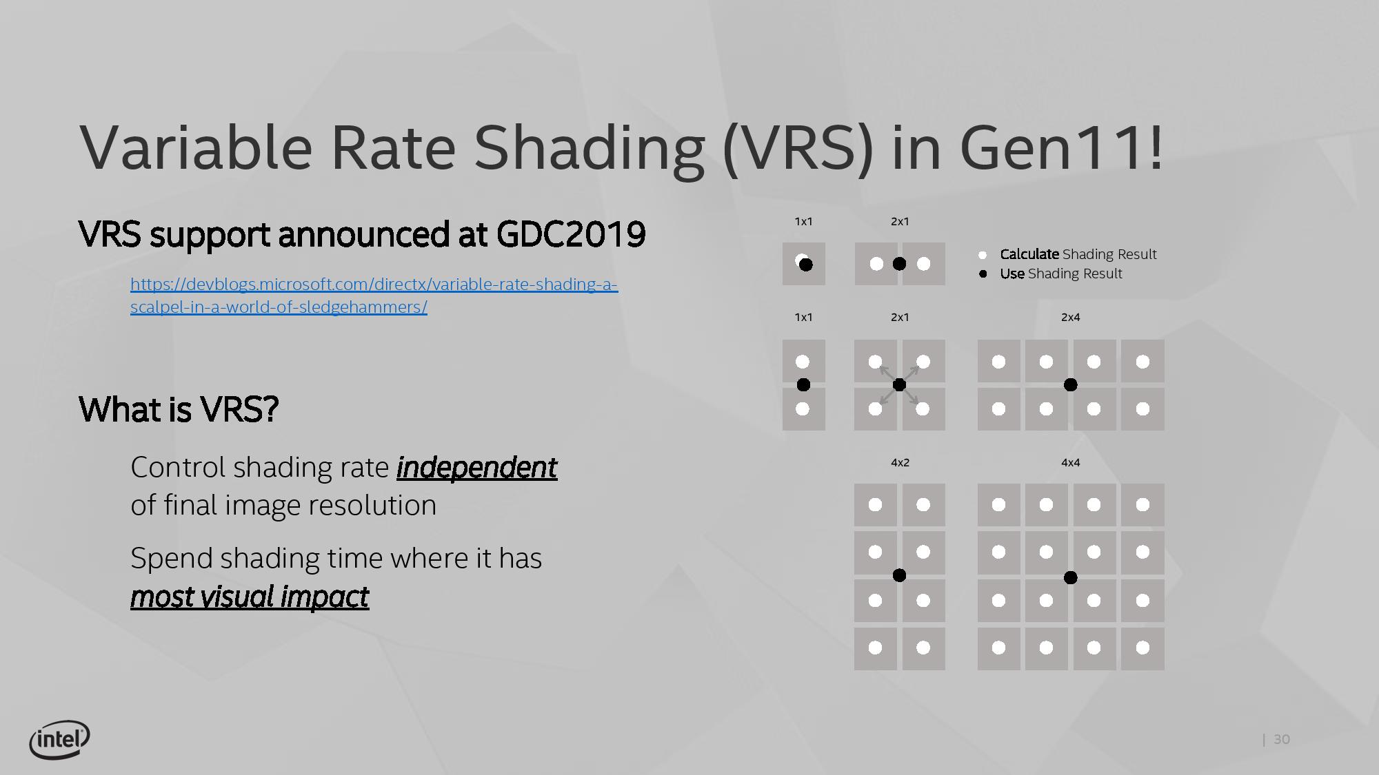
The idea is that using this method can reduce some of the load on the execution units, ultimately increasing the frame rate. The size of that combination of pixels can be adjusted on a per-frame basis as well, allowing the game to take advantage of processing budget where it exists, or pull back to a point where performance is needed. Ultimately Intel believes that any image quality loss is not noticeable, especially for the performance impact they expect it to provide. Intel states that this technology is useful for areas such as lighting adjustments, partially obscured objects (by fog/clouds), and areas that undergo blur, or foveated rendering – basically any area where clarity isn’t explicitly required to begin with.
The only issue here though is an ecosystem one – it requires the game developer support. Intel is already working with Epic to add it to the Unreal Engine, and Intel has worked with developers to enable support in titles such as Civilization 6. The difference in performance, according to Intel, can be up to a 30% FPS increase in a best-case scenario. NVIDIA already supports VRS through dedicated hardware, whereas AMD’s current solutions are best described as a more limited shader-based approximation.


107 Comments
View All Comments
repoman27 - Tuesday, July 30, 2019 - link
“Each CPU has 16 PCIe 3.0 lanes for external use, although there are actually 32 in the design but 16 of these are tied up with Thunderbolt support.”This isn’t quite right. The ICL-U/Y CPU dies do not expose any PCIe lanes externally. They connect to the ICL PCH-LP via OPI and the PCH-LP exposes up to 16 PCIe 3.0 lanes in up to 6 ports via HSIO lanes (which are shared with USB 3.1, SATA 6Gbps, and GbE functions). So basically no change over the 300 Series PCH.
The integrated Thunderbolt 3 host controller may well have a 16-lane PCIe back end on-die, and I’m sure the CPU floorplan can accommodate 16 more lanes for PEG on the H and S dies, but that’s not what’s going on here.
voicequal - Friday, August 2, 2019 - link
The SoC architecture shows a direct path for the Thunderbolt3 PCIe lanes to the CPU, with only USB2 going across OPI.. Whatever PCIe lanes are available on the PCH are in addition those available via TB3.https://images.anandtech.com/doci/14514/Blueprint%...
repoman27 - Tuesday, August 6, 2019 - link
The Thunderbolt 3 controller is part of the CPU die. There are four PCIe 3.0 x4 root ports connected to the CPU fabric that feed the Thunderbolt protocol converters connected to the Thunderbolt crossbar switch (the Converged I/O Router block in that diagram). The CPU exposes up to three (for Y-Series) or four (for U-Series) Thunderbolt 3 ports. The only way you can leverage the PCIe lanes on the back-end of the integrated Thunderbolt 3 controller is via Thunderbolt.The PCH is a separate die on the same package as the CPU die. The two are connected via an OPI x8 link operating at 4 GT/s which is essentially the equivalent of a PCIe 3.0 x4 link. The PCH contains a sizable PCIe switch internally which connects to the back-ends of all of the included controllers and also provides up to 16 PCIe 3.0 lanes in up to 6 ports for connecting external devices. These 16 lanes are fed into a big mux which Intel refers to as a Flexible I/O Adapter (FIA) along with all the other high-speed signals supported by the PCH including USB 3.1, SATA 6Gbps, and GbE to create 16 HSIO lanes which are what is exposed by the SoC. So there are up to 16 PCIe lanes available from the Ice Lake SoC package, all of which are provided by the PCH die, but they come with the huge asterisk that they are exposed as HSIO lanes shared with all of the other high-speed signaling capabilities of the PCH and provisioned by a PCIe switch that effectively only has a PCIe 3.0 x4 connection to the CPU.
This is not at all what Ian seemed to be describing, but it is the reality.
And the USB 2.0 signals for the Thunderbolt 3 ports do indeed come from the PCH, but they do not cross the OPI, they're simply routed from the SoC package directly to the Thunderbolt port. The Thunderbolt 3 host controller integrated into the CPU includes a USB 3.1 xHCI/xDCI but does not include a USB 2.0 EHCI.
poohbear - Tuesday, July 30, 2019 - link
I was looking at buying Dell's XPS 15.6" (7590 model), but with Project Athena laptops a few months away, i think i'll wait. Intel parts for solid reliability and unified drivers, and "4 hours of battery life with <30min of charging", those 2 on their own make the wait worth it for me!repoman27 - Tuesday, July 30, 2019 - link
“The connection to the chipset is through a DMI 3.0 x4 link...”Should be OPI x8 for U/Y Series.
“...Ice Lake will support up to six ports of USB 3.1 (which is now USB 3.2 Gen 1 at 5 Gbps)...”
They’re USB 3.1 Gen 2 ports, so it’s six USB 3.2 Gen 2 x 1 (10 Gbit/s) ports.
Roel9876 - Tuesday, July 30, 2019 - link
Well, for one, it is certainly not realistic to run single thread benchmarks on application that support multi threading. Realistically, most (all?) people will run the application multi threaded?HStewart - Tuesday, July 30, 2019 - link
As developer for many years, multiple threads are useful for handling utility threads and such - but IO is typically area which still has to single thread. Unless it has significantly change in API, it is very difficult to multi-thread the actual screen. And similar for disk io as resource.Arnulf - Tuesday, July 30, 2019 - link
"Our best guess is that these units assist Microsoft Cortana for low-powered wake-on voice inference algorithms ..."Our best guess is that these are designed for use by assorted three-letter agencies.
PeachNCream - Tuesday, July 30, 2019 - link
Open mics are totally okay. There is absolutely no privacy risk to you at all and you should never give it a second thought.ToTTenTranz - Tuesday, July 30, 2019 - link
With 4x TB3 connections available, I wonder if the maker of an external GPU box could develop a multiplexer that combined two TB3 connections into a PCIe 3.0 8x.This would significantly decrease some problems that eGPU owners are having due to relatively low CPU-GPU bandwidth.