Arm Announces Neoverse N1 & E1 Platforms & CPUs: Enabling A Huge Jump In Infrastructure Performance
by Andrei Frumusanu on February 20, 2019 9:00 AM ESTFirst N1 Silicon: Enabling the Ecosystem with SDPs
A little known fact about Arm is that the company designs its own silicon test platform – actually deploying them on development board to enable validation and software development on hardware that Arm and developers have full control of. The latest generation was the Juno platform, which in its first revision started off with a Cortex A57 and served as the fundamental silicon testbed for ARMv8 software.
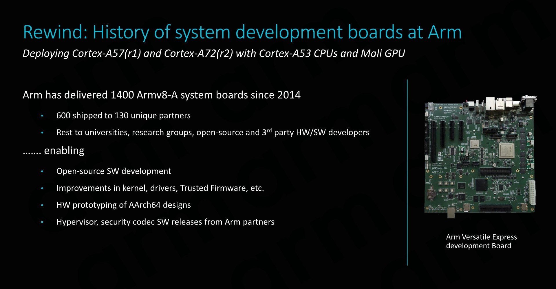
Ever since Arm started the programme in 2014, Arm has shipped over 1400 boards both internally and to its partners. The amount of chips we’re talking about here sounds paltry, however we have to keep in mind we’re talking about very limited shuttle runs on MPW (multi-project wafers) where Arm shares wafer space with numerous other companies.
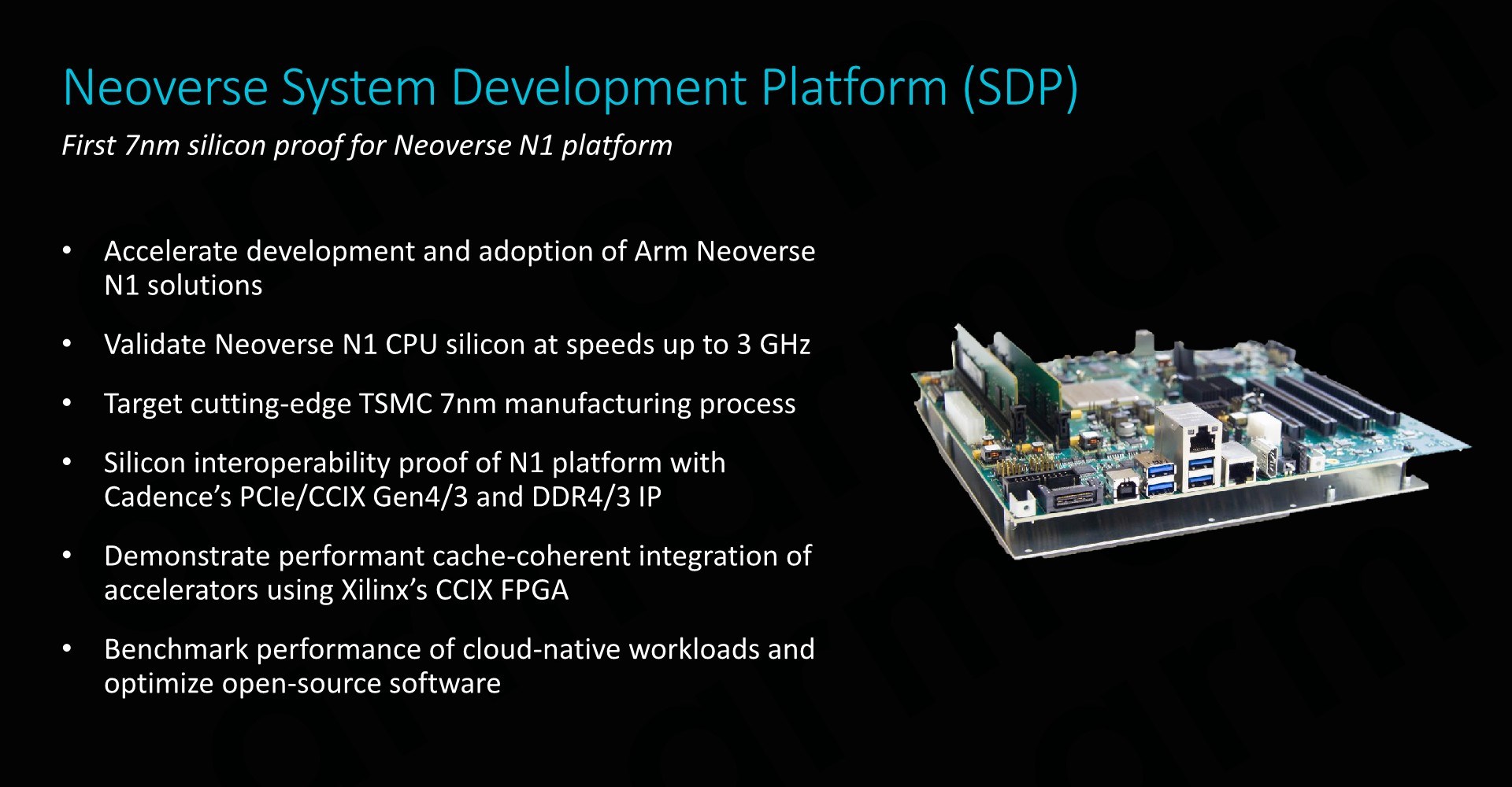
For today’s announcement, Arm had the pleasure to reveal that it received back the first working Neoverse N1 silicon back in December – with the chips meant to be integrated into the new Neoverse System Development Platform (SDP).
The N1 SDP represents major step for Arm as it not only is the first silicon to come back with the N1 CPU, but also is Arm’s first own 7nm silicon. The platform represents a major proof of concept of the IP, as well as interoperability with third-party IP, employing a lot of the peripheral IP such as PCIe and DDR PHY supplied by Cadence.
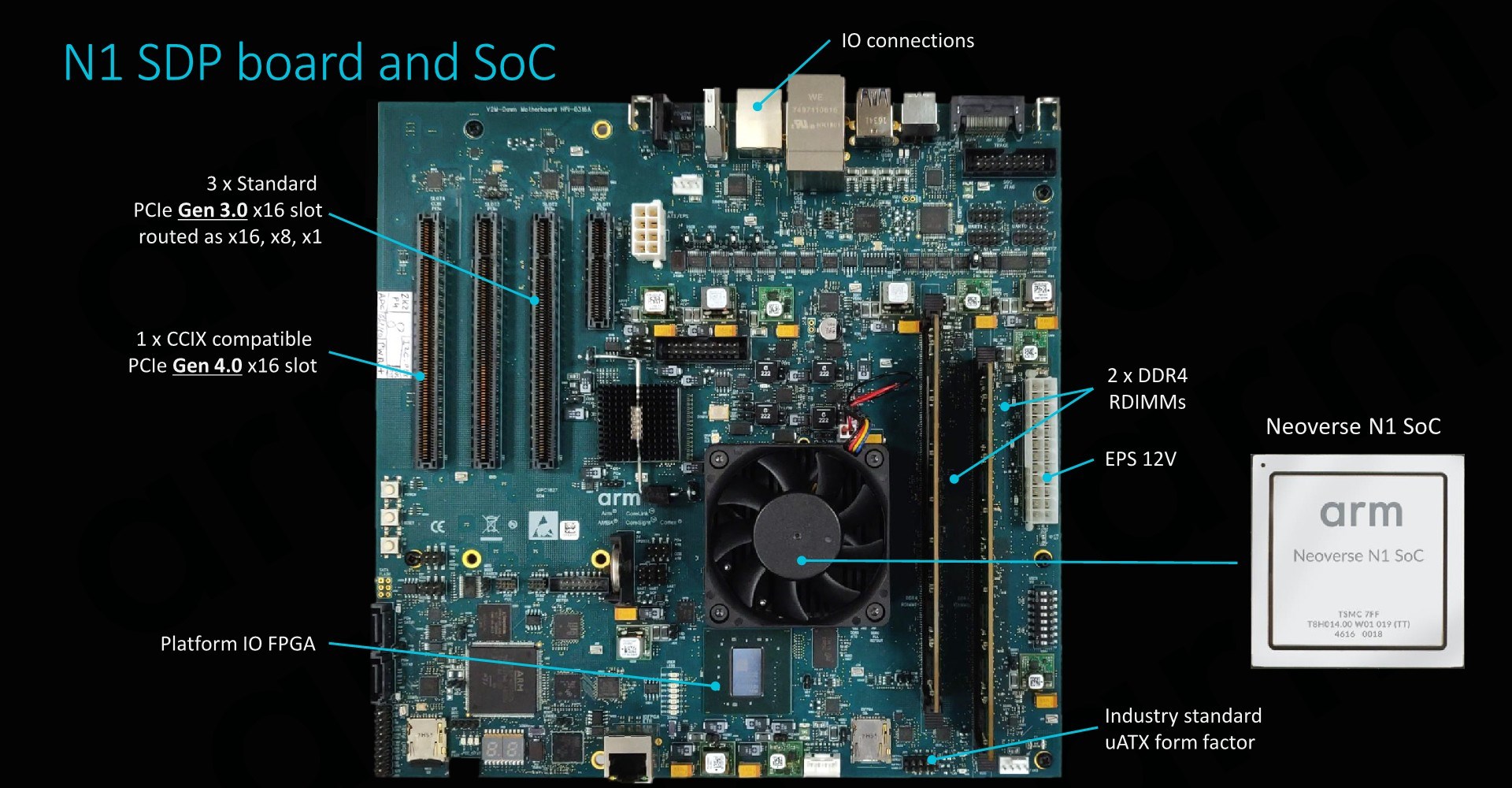
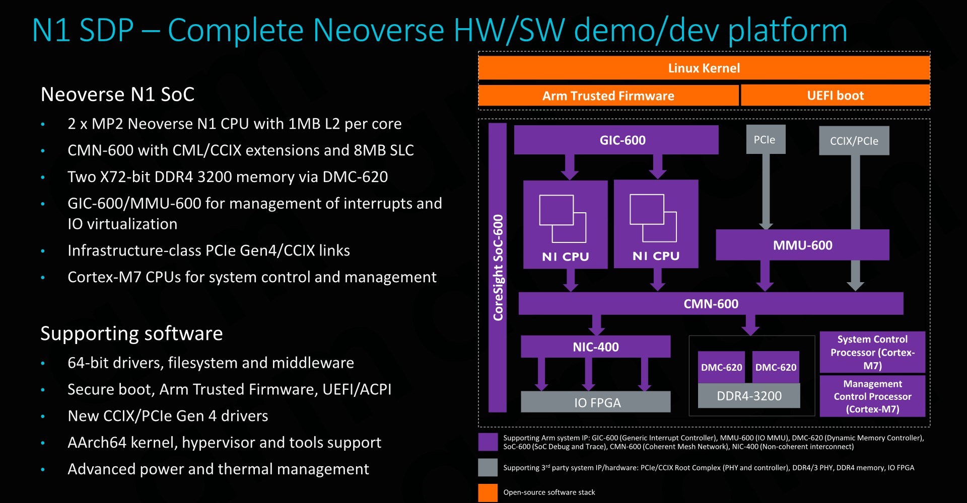
The actual hardware is a limited implementation of an N1 SoC – we find a 4-core N1 CPU with 1MB L2 configuration in the form of 2xMP2 connected to a CMN-600 with an 8MB SLC setup.
The board includes a CCIX compatible PCIe 4.0 x16 slot which serves the crucial role of enabling development and demonstrating cache-coherent integration with CCIX hardware such as Xilinx’s FPGA.
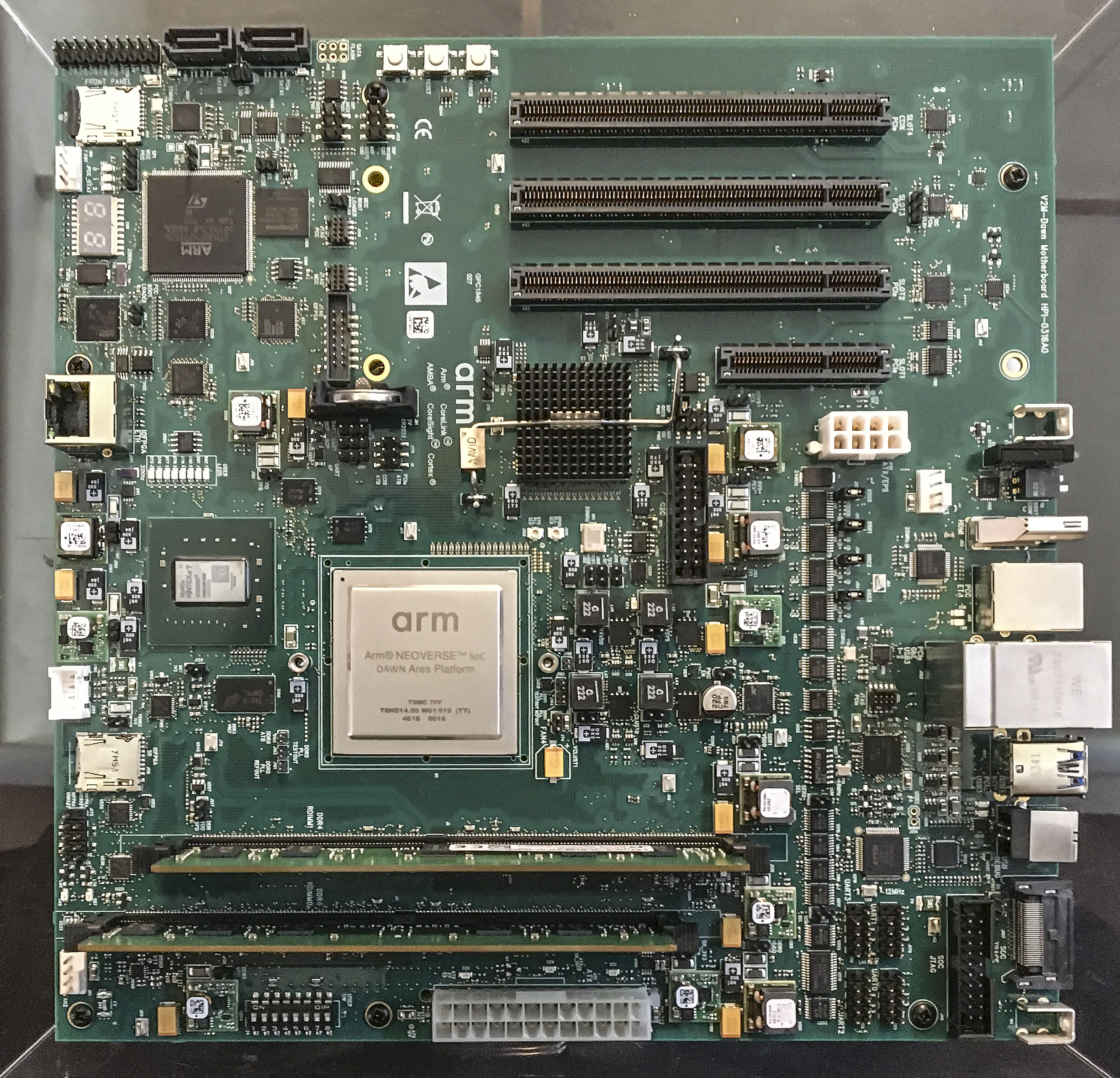
The N1 SoC actually doesn’t contain dedicated I/O IP, rather Arm implements all connectivity via a dedicated FPGA which serves as the I/O hub, supporting various connectivity options such as Ethernet, USB, SATA and so on.
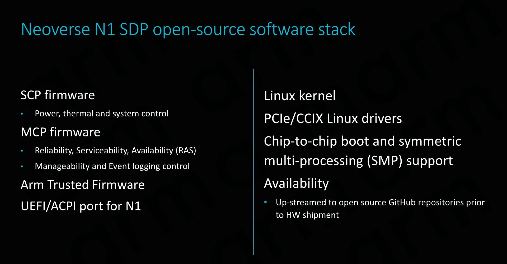
Naturally the big selling point of the SDP is its completely open-source firmware stack from not only the OS drivers, but more importantly the SCP and MCP firmware.
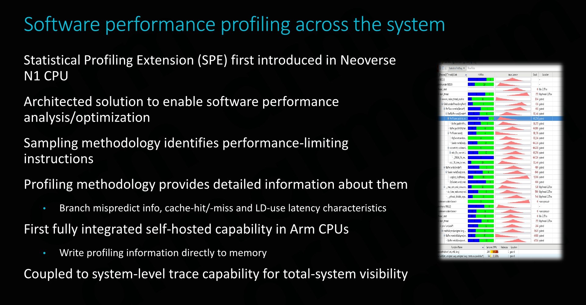
An important new feature that is first employed by the new N1 CPU is the introduction of statistical profiling extensions (SPE). The new extension enables the first ever self-hosted profiling capability in an Arm CPU – meaning we don’t require a separate CPU or system having to read out microarchitectural counters. Instead the new SPE can be configured to directly write this information into memory. The tool is extremely useful for tracing code and analysing core behaviour, identifying possible performance issues and further squeezing out the maximum performance out of a platform, something Arm is taking very seriously if it wants to succeed and gain adoption in HPC.
Finally, the N1 SDP will be available later this quarter – although don’t expect the board to be easily attainable for the average user.


101 Comments
View All Comments
lightningz71 - Thursday, February 21, 2019 - link
This is one I can answer. My computer engineering professors fielded this exact question. Essentially, when profiling code that was being used in modern software, the major CPU vendors realized that a small portion of the x86 instructions were rarely used. So rarely, in fact, that it was an absolute waste of silicone to try to implement them in hardware as it would be so rarely used. Add in that a lot of those instruction are not executed in isolation, but have some sort of dependency on fetching a piece of data, or waiting on the resolution of multiple intermediary steps during their execution, that going with full hardware implementations would not have resulted in a major boost in their performance. Instead, they elected to implement them in micro-code and execute them on the highly tuned circuits that they used to implement the more common instructions in the back end. So, while you loose some performance having to load and run the microcode sequences, its actually executing those simplified sub-instructions very rapidly, and can do other things while waiting for various tasks to complete.so, while there is a case to be made that a full, tuned and optimized hardware implementation of the more complex instructions can be done, and perform more quickly than the micro-code sequences, the actual speedup for the overall performance of the systems in question would be minimal because of how rarely those actual instructions are used in practice. You're talking about shaving off a few tens of cycles per instance on a processor that is running at around 4Ghz these days. The real performance impact would be minimal, but the development cost and circuit budget consumed would be significant for not much gain.
FunBunny2 - Thursday, February 21, 2019 - link
"Essentially, when profiling code that was being used in modern software, the major CPU vendors realized that a small portion of the x86 instructions were rarely used. "not to do too much what-about-ism, but IBM was doing that with COBOL applications, in real time monitoring (allowance to do so was embedded in the lease agreement), at least as early as the 360.
naturally, I didn't remember that lower brain stem memory until reading your comment. my shame. (:
but... I do wonder about all those 'extensions' to the original 8086 instruction set. weren't they created to support 'necessary' functions? here: https://en.wikichip.org/wiki/x86/extensions
or are they, too, not used enough?
Wilco1 - Thursday, February 21, 2019 - link
Well when did you last use MMX? Or x87 floating point? There are large numbers of instructions which are hardly ever used.FunBunny2 - Thursday, February 21, 2019 - link
HLL coders don't, at least directly. but I'm old enough to remember when adding a '87 (before FP was moved to the '86) put a rocket under 1-2-3.Wilco1 - Thursday, February 21, 2019 - link
The point is both have been superceded by all the SSE variants which itself is now being replaced by AVX. Intel has posted patches to change HLL MMX intrinsics to use SSE instructions instead of MMX.zmatt - Wednesday, February 27, 2019 - link
Usually you don't invoke those yourself. The compiler does.nevcairiel - Wednesday, February 20, 2019 - link
The desktop and notebook market will face adoption problems simply from having your software run (fast). Of course they can use emulation layers, but that once again costs you efficiency/performance.Mobile was an entirely new space, so no pre-existing software to really worry about, and servers are a far more managed space so that software is often more readily available in the variants you need. Desktop usages on the other hand are full of legacy software that has to work.
ZolaIII - Wednesday, February 20, 2019 - link
In it's core (integer base instruction set) it is more efficient but that doesn't mean much nowadays. Main factor is design of actual core as such.ballsystemlord - Wednesday, February 20, 2019 - link
But, and here's the kicker, the binary nature of proprietary SW means that switching arches will require many fixes to programs and many more will never be ported. Emulation, which is slow for CPU arches, is the only way that such SW could continue to exist.Gee, Stallman was wright!
wumpus - Thursday, February 21, 2019 - link
Put it this way: the effective means to convert a "CISC" architecture to internally* "RISCY" operation could be included on a CPU core effectively in the mid 1990s. This pipeline step is sufficiently small to make no difference nowadays (although Sandy Bridge and later use caches to store pre-decoded micro-ops). The RISC/CISC wars died a long time ago, and now we only have Intel vs. ARM vs. AMD (and don't forget IBM).* (Internally RISC). Oddly enough, the more "internally RISCy" a 1990s-era chip was the less successful it was. The AMD K5 was internally a 29k derivative (a real RISC) and failed miserably. Supposedly IBM had a PowerPC/X86 hybrid that never made it out of the lab. Transmeta did its translation in software, but fell into the "single device power trap". Nextgen was probably more successful than all of these (especially in convincing AMD to buy them and producing the mighty Athlon), and had the ability to execute native code (supposedly. I don't think anyone ever did. Presumably involved 80 bit instructions). Pentium Pro, K6, Pentiums 2&3, Athlon all executed "native microcodes" but don't appear to slavishly copy RISC dogma.