Arm Announces Neoverse N1 & E1 Platforms & CPUs: Enabling A Huge Jump In Infrastructure Performance
by Andrei Frumusanu on February 20, 2019 9:00 AM ESTE1 Implementation & Performance Targets
The Neoverse E1 CPU being a small CPU core aimed at cost-effective and dense implementation naturally needs to be quite small, as well as power efficient.
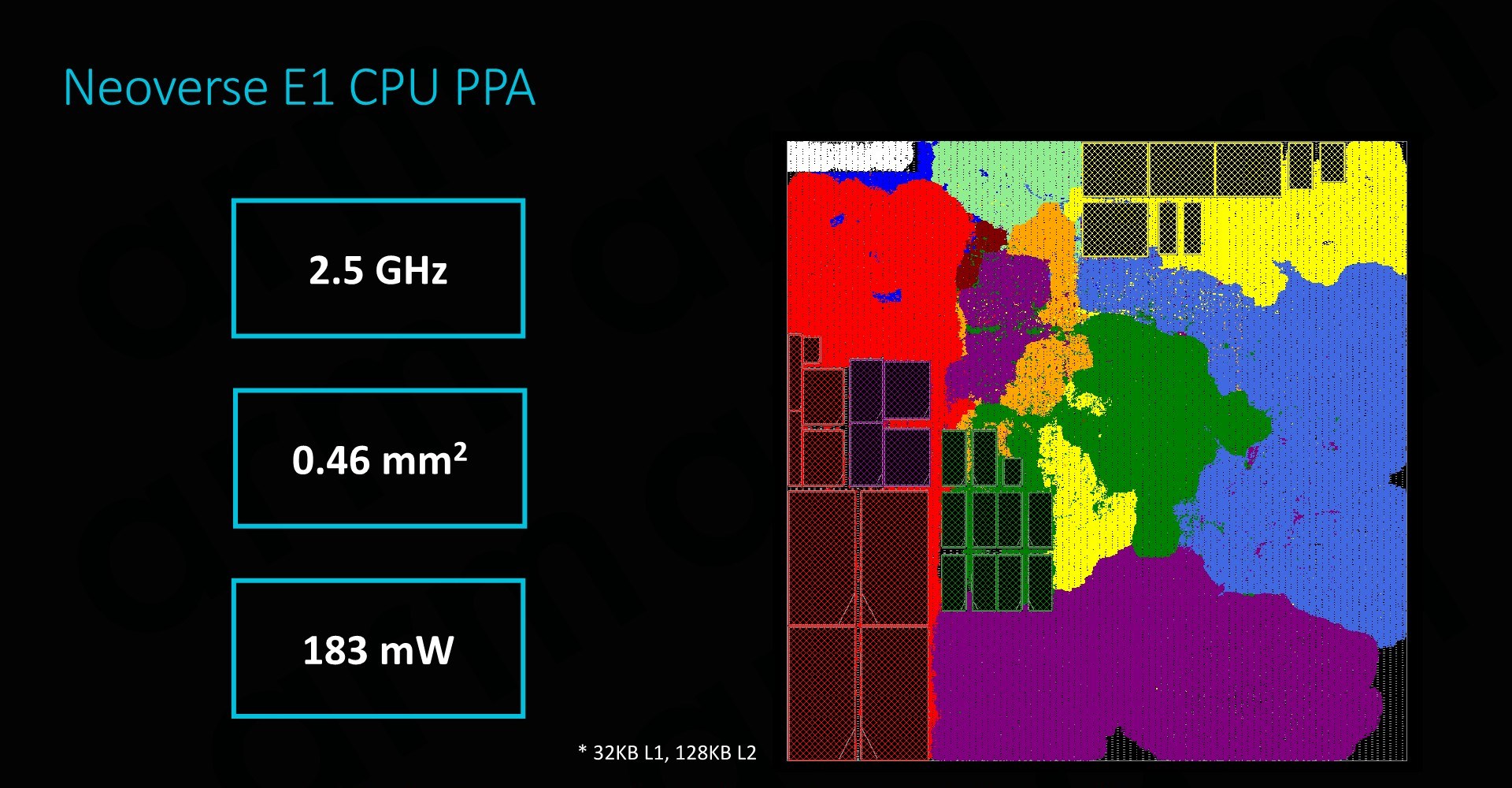
Implemented on a 7nm process, Arm physical design team is able to get an E1 CPU core with 32KB L1 and 128KB L2 cache down to 0.46mm² - all while reaching a high clock of 2.5GHz and a power consumption of 183mW. The higher clock was a surprise as it is quite notably higher than what we’ve seen vendors achieve on the A55 – although we are talking about different implementation targets.
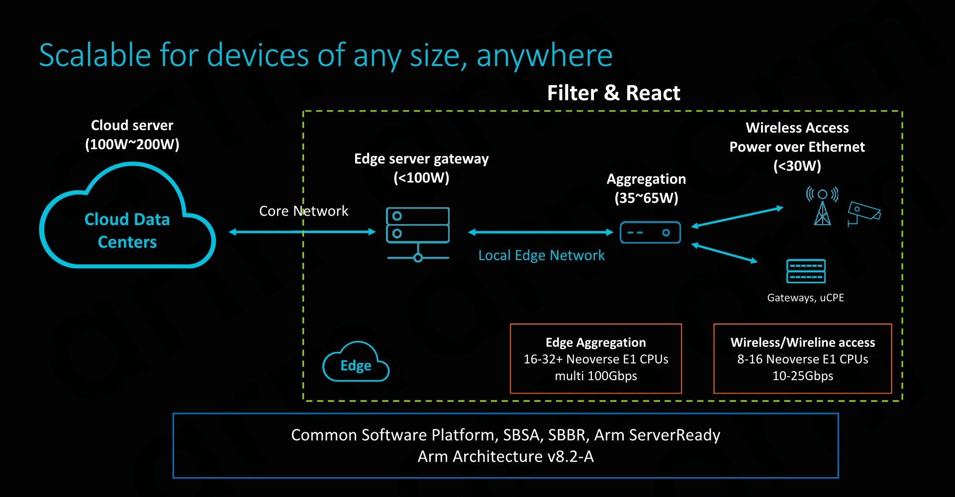
Arm envisions the most popular implementations of the E1 to be found in lower power edge applications. At the lower end, ranging from 8-16 cores would be a good for wireless access points and gateways, delivering data throughputs in the 10-25Gbps rang. A tier up we would see 16-32 core designs in use-cases such as edge data aggregation deployments, achieving data rates in the 100’s of Gbps.
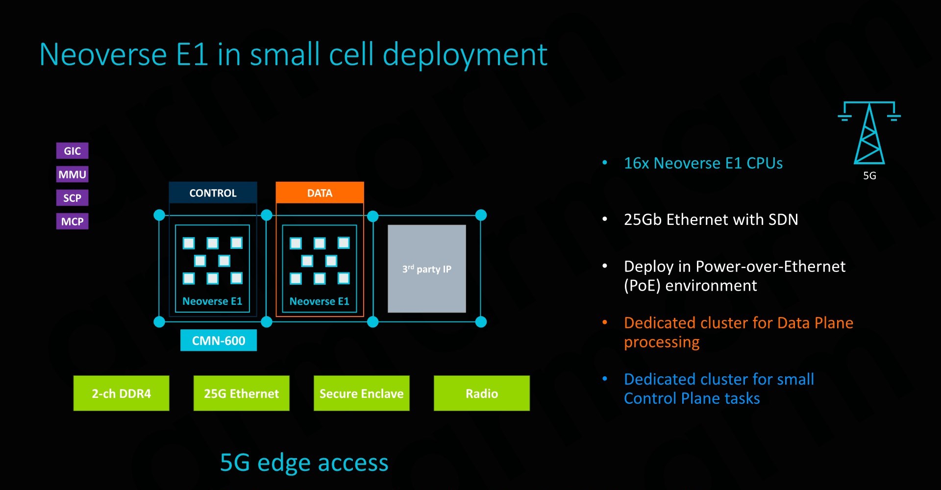
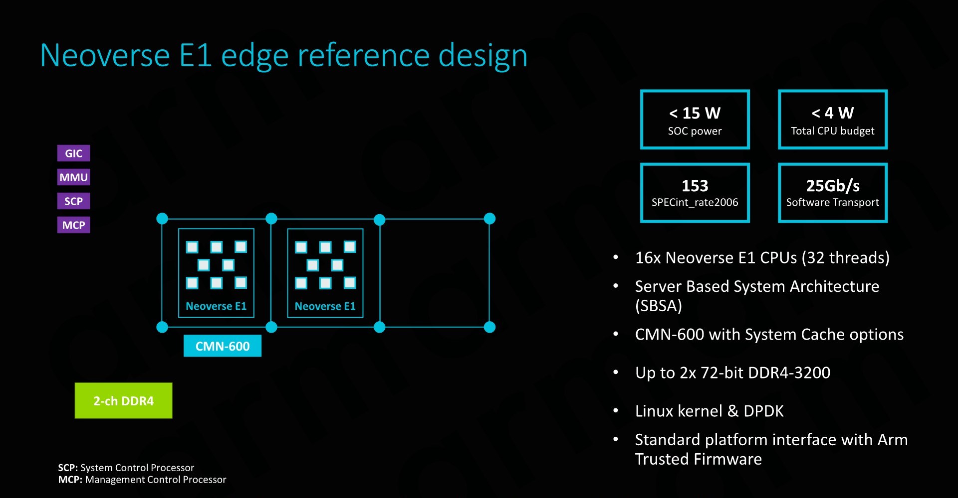
The Neoverse E1 reference design that Arm offers and sees as being the most popular “sweet-spot” is based on a 16 core design. Here we have to clusters of 8 cores in a small CMN-600 2x4 mesh network, allowing for system cache options as well as integration of possible additional third-part IP. The envisioned memory system would be a 2-ch DDR4 configuration.
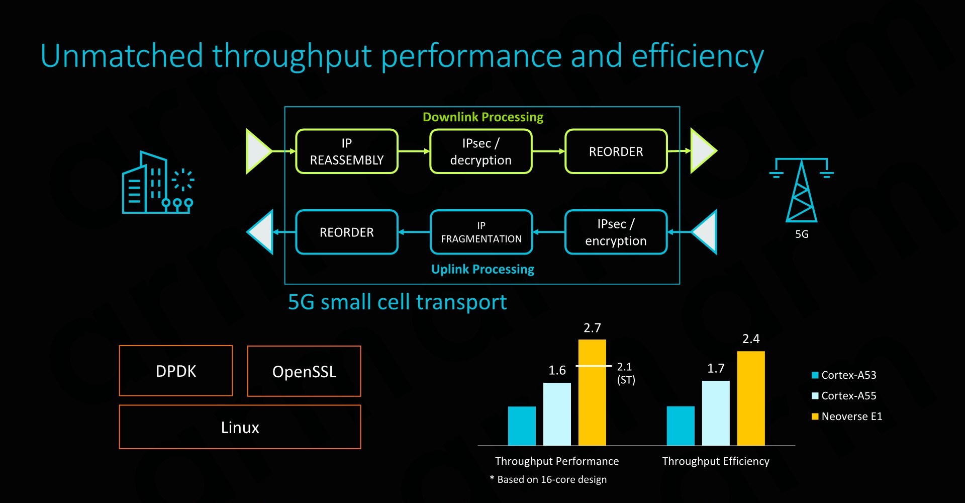
Such as SoC would have a power consumption of less than 15W, of which less than 4W would actually be used by the CPU cores. SPECint2006 rate scores would come in at 153 – which given the actual size and power consumption of the platform is quite impressive. The system would also be capable of 25Gb/s network throughput, enabled solely by a software transport layer (Meaning no hardware acceleration).
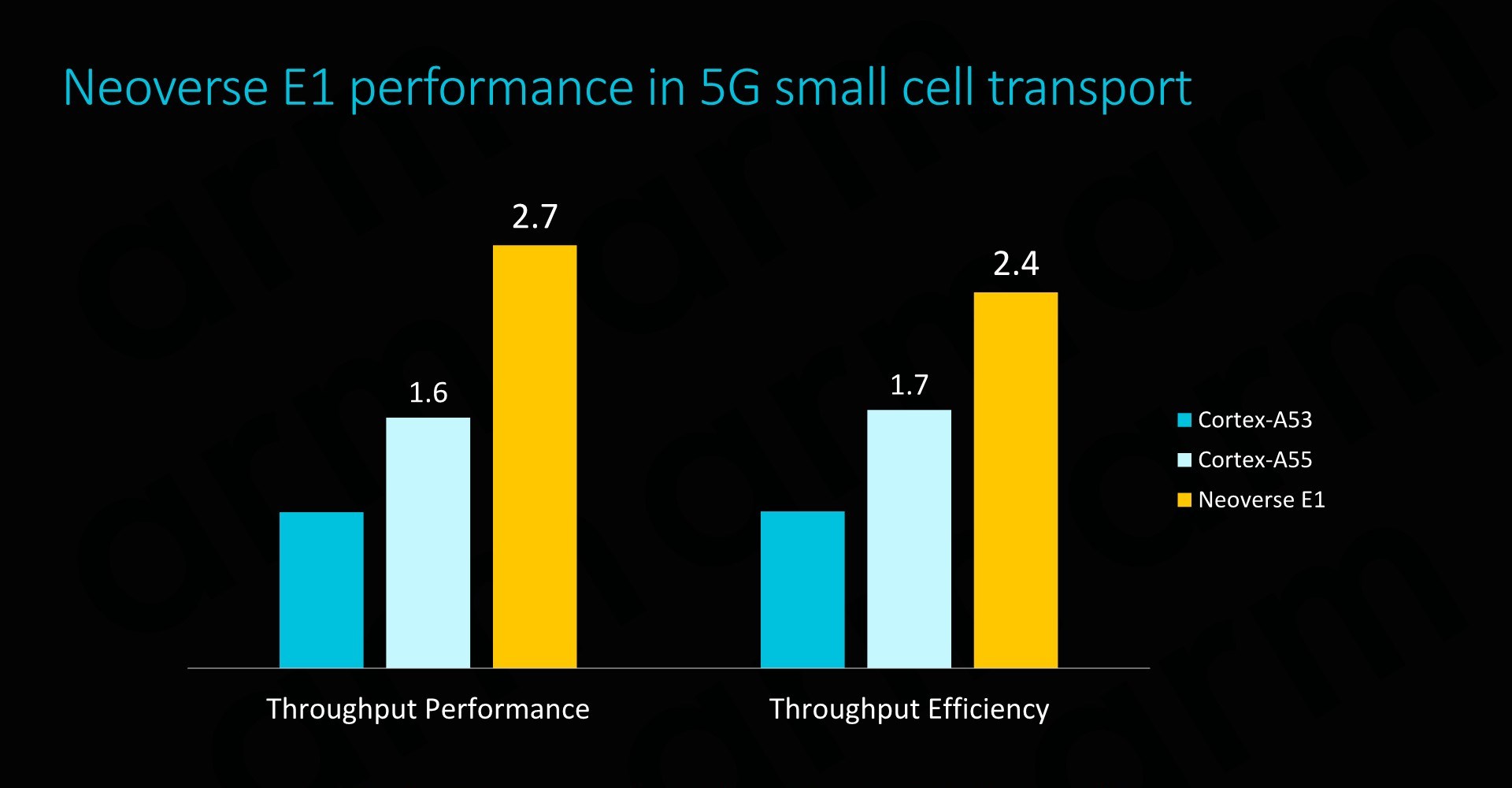
On a per-core comparison to the Cortex A53 and A55, the new E1 CPU would again offer significant throughput performance benefits, but also very importantly it would represent an efficiency boost compared to its predecessors (ISO process comparison).


101 Comments
View All Comments
WinterCharm - Wednesday, February 20, 2019 - link
There's a gigantic Arm vs x86/64 battle brewing for the entire computer industry. ARM is just more efficient at every level, and if software is properly optimized it performs brilliantly.eva02langley - Wednesday, February 20, 2019 - link
However, it doesn't have the raw power required for many fields like scientific, compute and research. The core-count is also a huge factor in the upcoming future and unless you develop a chiplet approach, ARM is going to face the same issue of monolithic chips.The next chiplet evolution will require stacking. The future is way more related to modularity than the chip architecture. Don't get me wrong, the more advancement, the better for everyone, but I don't believe ARM is going to render x86 obsolete, hovwever I believe multi-chips SoC are going to render monolithic chip obsolete in the computer world.
SarahKerrigan - Wednesday, February 20, 2019 - link
Sure it does. There are ARM supercomputers, and this very article shows an N1 core outperforming Zen on single-thread, and both Zen and SKL-SP on throughput.HStewart - Wednesday, February 20, 2019 - link
I think you are forgetting the very nature of RISC (Arm) vs CISC (x86) architectures. By the nature of designed of RISC - reduce instruction set, it takes more instruction to execute same operation than CISC. For simple stuff RISC can likely do better but remember also modern x86 based CPU also break down more complex instructions in simpler instruction so it can run one multiple pipelines.SarahKerrigan - Wednesday, February 20, 2019 - link
Dude, I work in the semi industry, and I've designed pipelined cores. Saying "ARM's workload-demonstrated higher performance doesn't matter because x86 is CISC" is idiotic.SPEC isn't "simple stuff." It is a selection of extremely compute-intensive workstation loads, one that the whole industry - including Intel - uses to demonstrate comparative performance.
HStewart - Wednesday, February 20, 2019 - link
The biggest thing I found that seems misinformation is statement that these are estimates and this chip is simulated which tells me they don't need the real numbers.All I am saying is that CISC instructions can do more than RISC instructions per instruction, and it depends on compiler to take advantage of the those instructions. Please note I never sated it does not matter and that was in your words. I just mention considerations need to take in account of different architextures and the fact they are comparing future simulated designed to last year designs.
Andrei Frumusanu - Wednesday, February 20, 2019 - link
> All I am saying is that CISC instructions can do more than RISC instructions per instructionNobody cares. If the performance per clock is same or higher, you're just arguing about semantics.
Internally CISC processors break things down into RISC like µOps anyway.
ZolaIII - Wednesday, February 20, 2019 - link
@Andrei Frumusanu what would be estimated size of an A55 core with similar amount of cache as on represented E1 on 7nm lithography? I am very curious about that one. Also comparation to the A72 & A73 should be a good thing as ARM clames it reaches their level of performance. Its very interesting first born (SMT) and much needed one.zmatt - Wednesday, February 20, 2019 - link
When people talk about complex instructions they don't mean something like find the derivative of x^2. They mean something like a conditional move operation. The speed advantages on paper between RISC and CISC are in theory a wash. This is because while CISC can conceivably do more in an instruction, RISC can do more instructions per clock generally. In the real world the simplicity of RISC means usually, all other things being equal, the chips are simpler and can run higher clocks, draw less power and generate less heat for a given level of performance.x86 chips haven't actually been CISC since the mid 90's. Both Intel and AMD have been making chips that take the CISC instructions and run them through an instruction decoder that then hands RISC instructions to the actual cpu. Yes this does incur some overhead but it frees up cpu design quite a bit without being so closely tied to backwards compatibility.
The fact that modern x86 chips ultimately are actually executing code as reduced instruction sets shows you don't understand the concept.
Wilco1 - Wednesday, February 20, 2019 - link
x86 is still a CISC ISA irrespectively of how it executes instructions. Note that compilers predominantly use the simpler instructions, rather than the microcoded instructions and that's why it's possible for x86 to be fast at all.