Arm Announces Neoverse N1 & E1 Platforms & CPUs: Enabling A Huge Jump In Infrastructure Performance
by Andrei Frumusanu on February 20, 2019 9:00 AM ESTFirst N1 Silicon: Enabling the Ecosystem with SDPs
A little known fact about Arm is that the company designs its own silicon test platform – actually deploying them on development board to enable validation and software development on hardware that Arm and developers have full control of. The latest generation was the Juno platform, which in its first revision started off with a Cortex A57 and served as the fundamental silicon testbed for ARMv8 software.
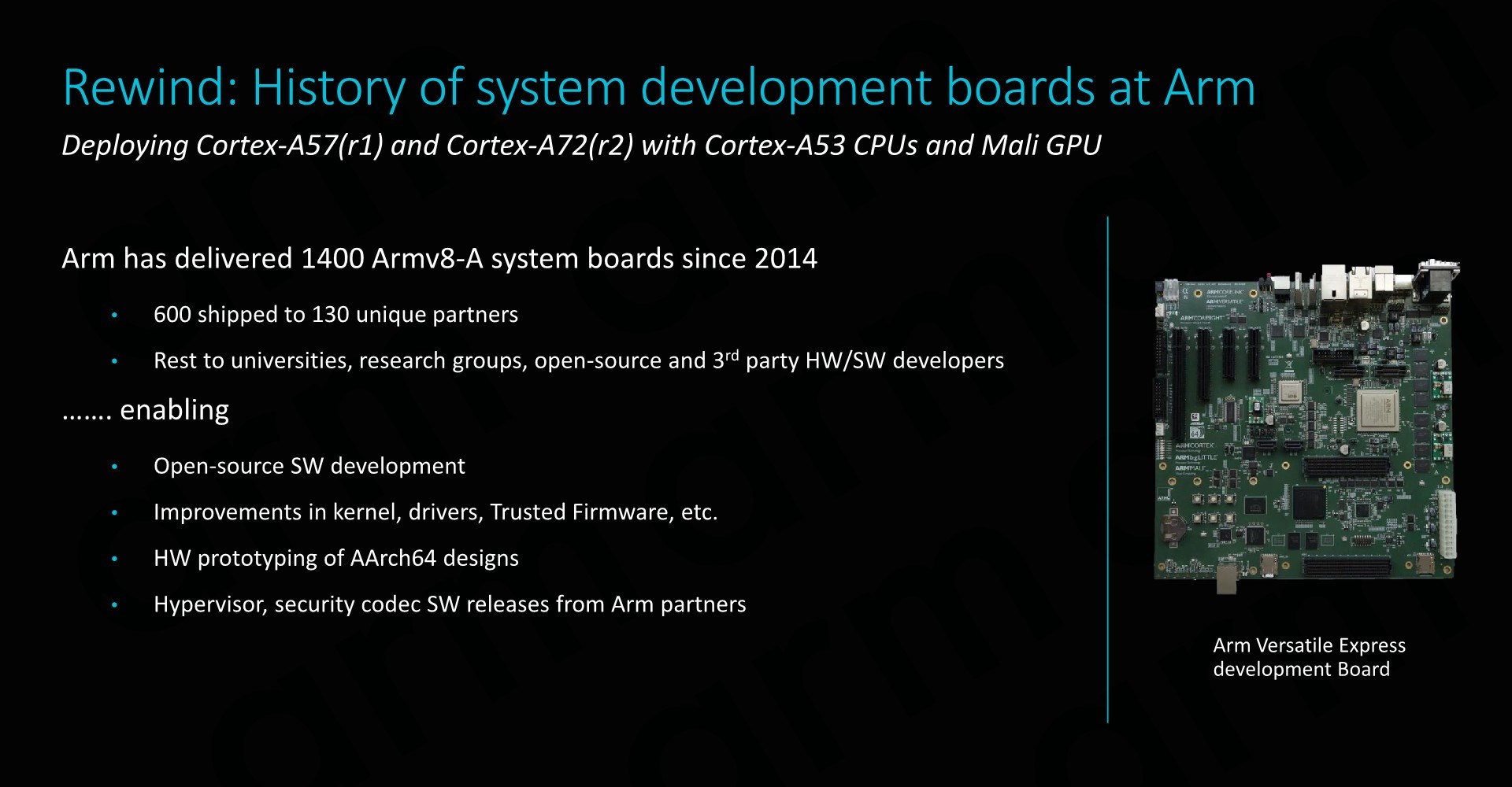
Ever since Arm started the programme in 2014, Arm has shipped over 1400 boards both internally and to its partners. The amount of chips we’re talking about here sounds paltry, however we have to keep in mind we’re talking about very limited shuttle runs on MPW (multi-project wafers) where Arm shares wafer space with numerous other companies.
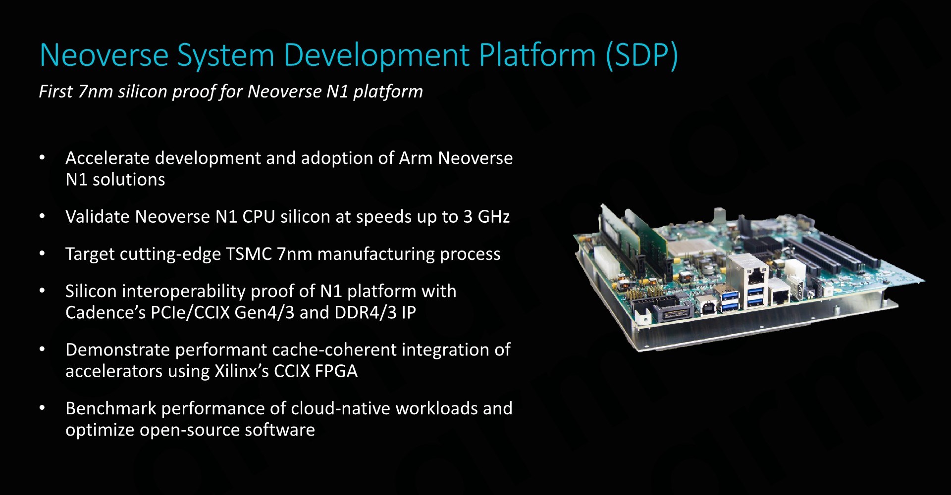
For today’s announcement, Arm had the pleasure to reveal that it received back the first working Neoverse N1 silicon back in December – with the chips meant to be integrated into the new Neoverse System Development Platform (SDP).
The N1 SDP represents major step for Arm as it not only is the first silicon to come back with the N1 CPU, but also is Arm’s first own 7nm silicon. The platform represents a major proof of concept of the IP, as well as interoperability with third-party IP, employing a lot of the peripheral IP such as PCIe and DDR PHY supplied by Cadence.
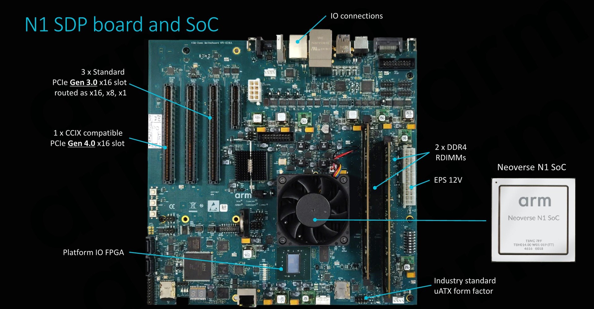
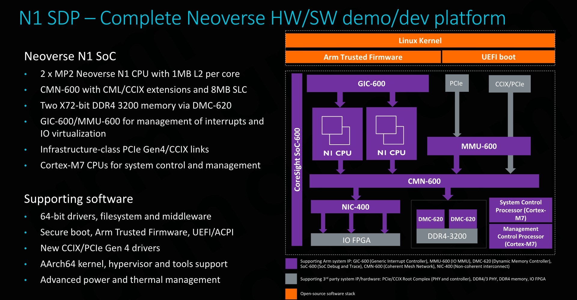
The actual hardware is a limited implementation of an N1 SoC – we find a 4-core N1 CPU with 1MB L2 configuration in the form of 2xMP2 connected to a CMN-600 with an 8MB SLC setup.
The board includes a CCIX compatible PCIe 4.0 x16 slot which serves the crucial role of enabling development and demonstrating cache-coherent integration with CCIX hardware such as Xilinx’s FPGA.
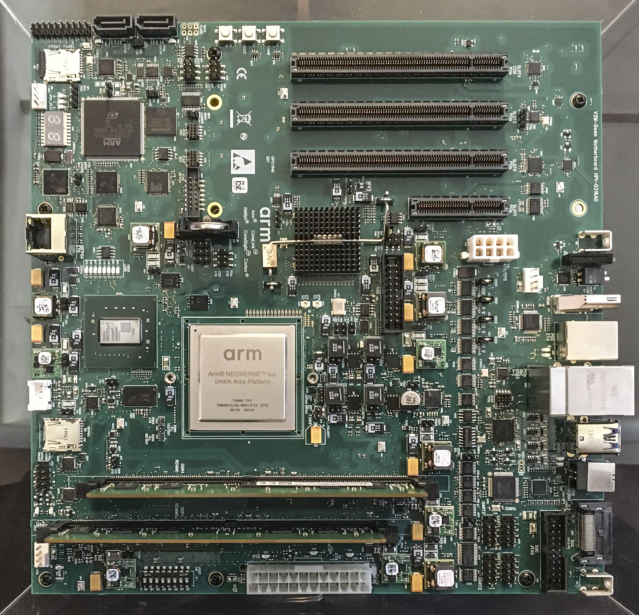
The N1 SoC actually doesn’t contain dedicated I/O IP, rather Arm implements all connectivity via a dedicated FPGA which serves as the I/O hub, supporting various connectivity options such as Ethernet, USB, SATA and so on.
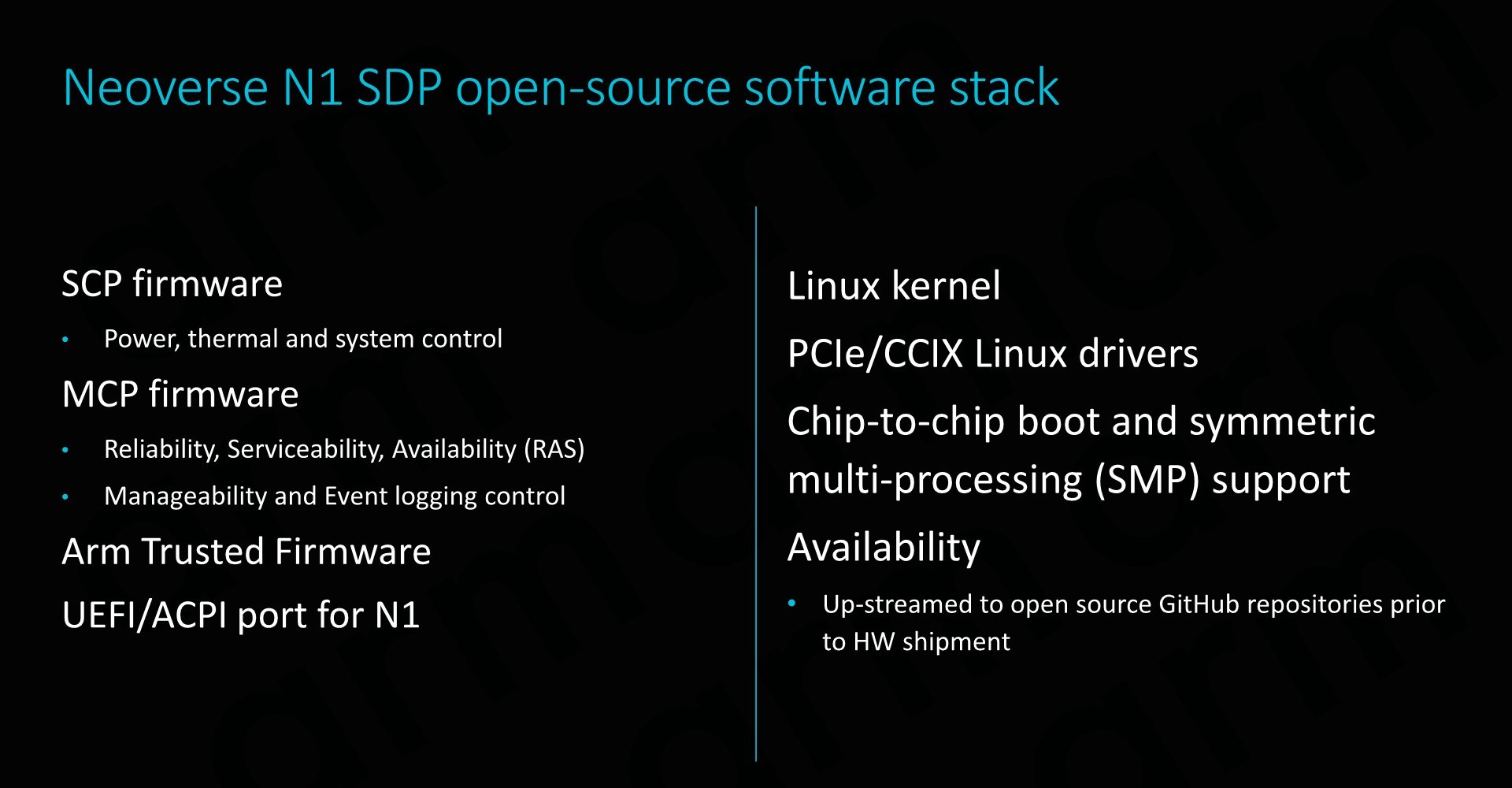
Naturally the big selling point of the SDP is its completely open-source firmware stack from not only the OS drivers, but more importantly the SCP and MCP firmware.
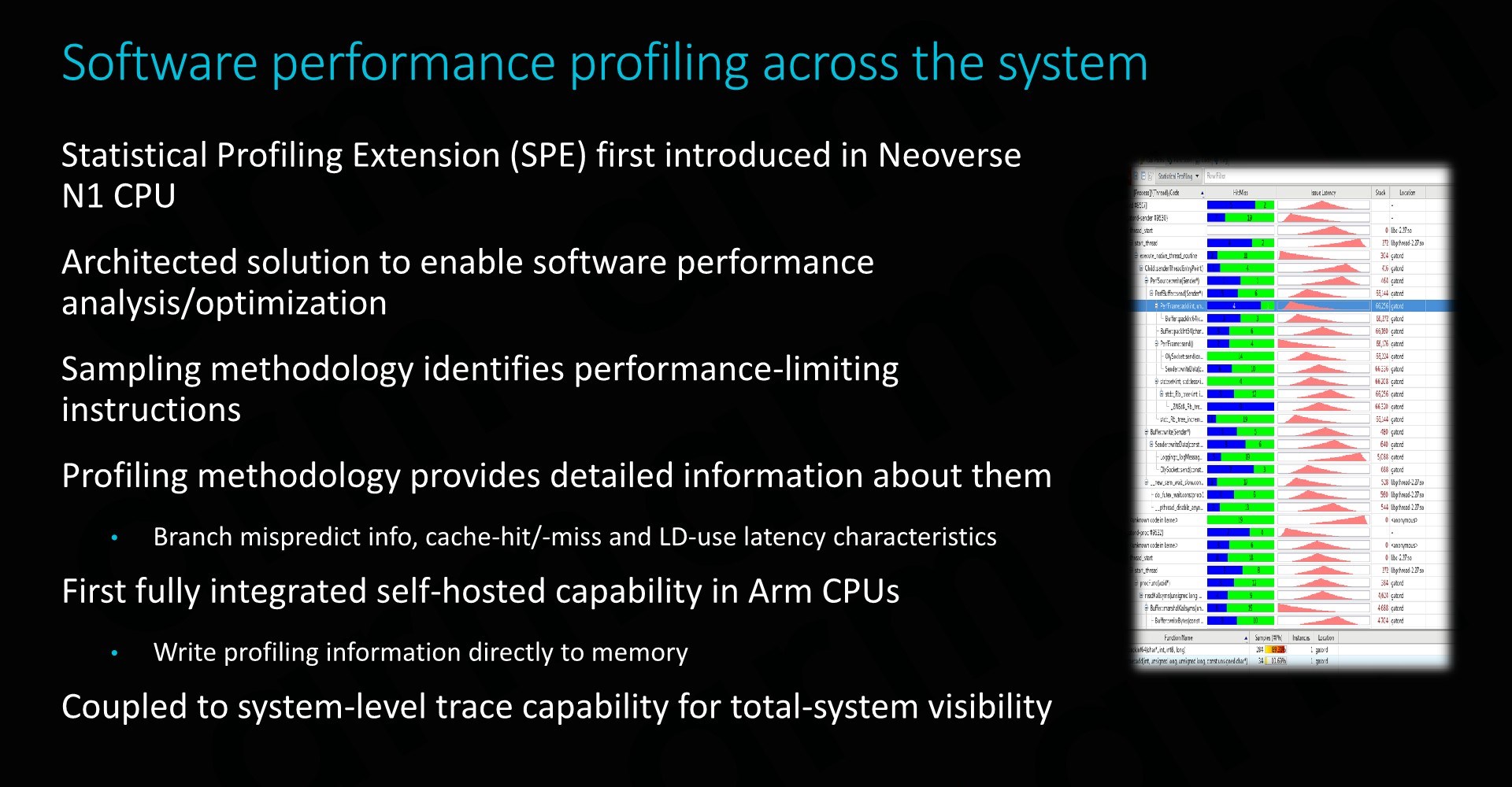
An important new feature that is first employed by the new N1 CPU is the introduction of statistical profiling extensions (SPE). The new extension enables the first ever self-hosted profiling capability in an Arm CPU – meaning we don’t require a separate CPU or system having to read out microarchitectural counters. Instead the new SPE can be configured to directly write this information into memory. The tool is extremely useful for tracing code and analysing core behaviour, identifying possible performance issues and further squeezing out the maximum performance out of a platform, something Arm is taking very seriously if it wants to succeed and gain adoption in HPC.
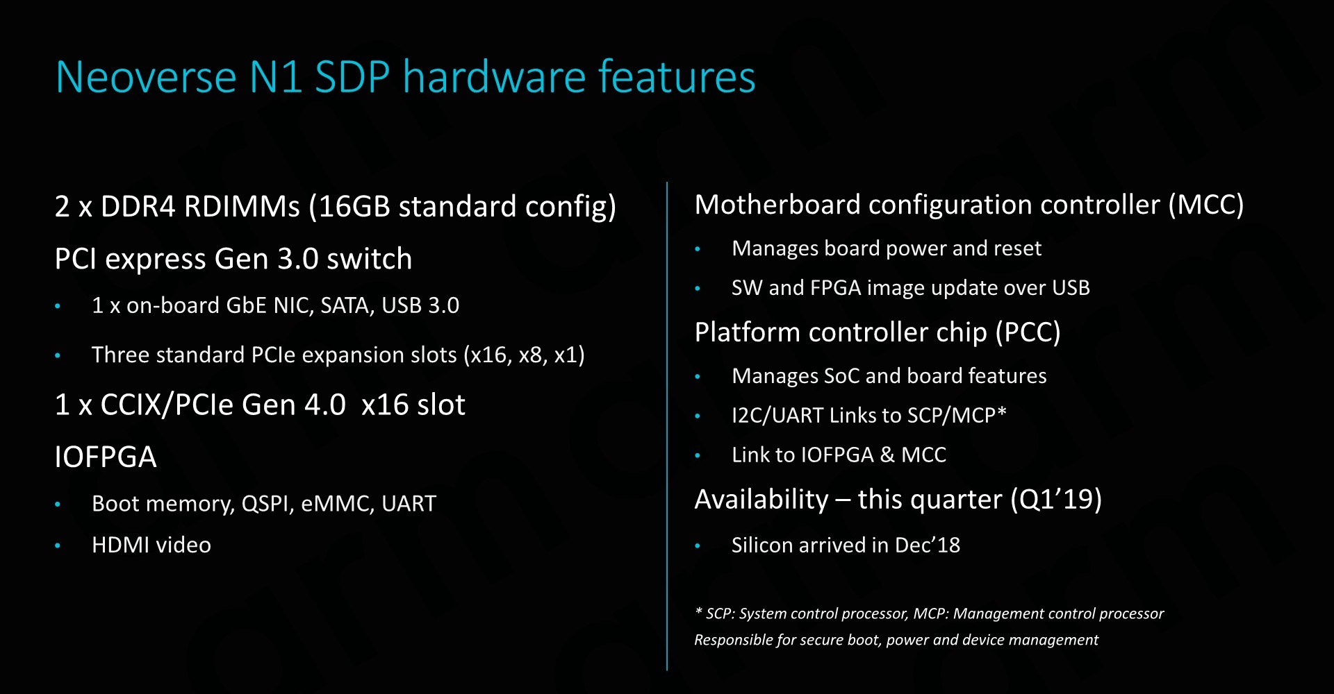
Finally, the N1 SDP will be available later this quarter – although don’t expect the board to be easily attainable for the average user.


101 Comments
View All Comments
Santoval - Thursday, February 21, 2019 - link
"Both Intel and AMD have been making chips that take the CISC instructions and run them through an instruction decoder that then hands RISC instructions to the actual cpu."The instruction decoder is also part of an "actual CPU". Beside the decoder the front-end also has instruction fetch, a branch predictor, predecode (potentially), μOP & L1 instruction cache, instruction queues, a TLB, allocation queues etc etc All these units are most certainly parts of the "actual CPU".
I believe you rather meant "hands RISC-like instructions to the *back-end* of the CPU".
FunBunny2 - Thursday, February 21, 2019 - link
"The speed advantages on paper between RISC and CISC are in theory a wash. "not to keep beating the dead horse 360, dated as it is, but with the hardware of the time (and IBM was the top of the heap, then) the 360/30 ran the instruction set in micro-code. allegedly the first computer to even have microcode. ran like drek compared to the all-hardware versions of the machine. the '30 real cpu was long reputed to be some DEC machine.
"cpu design quite a bit without being so closely tied to backwards compatibility."
lots of folks say that, but makes no sense to me. compilers target the instruction set, which only changes when Intel publishes 'extensions'. whether those instructions are executed in pure ISA hardware, or a rat running in a spinning wheel (RISC), makes no difference to the compiler writer.
the profiling explanation for microcode over pure ISA hardware makes the most sense.
Wilco1 - Wednesday, February 20, 2019 - link
The only misinformation is from you. RTL simulation is widely used in the industry and is quite accurate.Studies have shown CISC instructions don't do more than RISC instructions - partly because compilers avoid CISC instructions, partly because CISC instructions are slow. That's why RISC works. But I wouldn't expect you to understand this.
FunBunny2 - Thursday, February 21, 2019 - link
"Studies have shown CISC instructions don't do more than RISC instructions "at least in the z world (and predecessors), there were/are some (I don't remember the count) of 'COBOL assist' instructions which were/are quite complex and were introduced to reduce the amount of times the COBOL coders had to 'drop down to assembler'. whether that's still true, I can't say.
DigitalVideoProcessor - Thursday, February 21, 2019 - link
CISC vs. RISC is a debate about instruction decode philosophy and it has almost zero bearing on the performance of a system. CISC machines reduce everything to RISC like operations. Saying one does more than another in a given clock is misinformation.melgross - Thursday, February 21, 2019 - link
Those wars are long over. No modern chip is either pure CISC or RISC. Those are long gone.Calin - Thursday, February 21, 2019 - link
SPECint, SPECfp, ... are "work done tasks" - what your're referring to was "MIPS" (or millions of instructions per second). This performance metric has lost its charm since internally x86 processors no longer use x86 instructions but large bundles of microoperations that are done in parallel and can be interleaved (so two instructions that follow each other are broken into micro operations which are reordered, and might be finalized in a different order).Kevin G - Thursday, February 21, 2019 - link
The thing is that real distinction of CISC vs. RISC is lost in their similar implementations: pipelined OoO parallel execution engines. While CISC encoding may* permit more operations to be contained within a single instruction but at the cost of having to decode that instruction into an optimal arrangement given the hardware. The price paid is in power consumption and complexity which may impact factors like maximum clock speed. In the era of many core and power limitations, these attributes are the foundation for RISC to have an edge over legacy CISC designs. Not to say that RISC architectures can't leverage instruction decoding either: expanding out the fields for registers to account for the larger rename register space is a simple procedure.Once chips begin parallel execution, the CISC advantage of doing more per instruction really starts to fall apart. The raw amount of work being done per cycle approaches the common limit of just how much parallelism can be extracted by an inherently serial stream of instructions. Arguably CISC designs can hit this sooner in terms of raw instruction count as the instruction stream is _effectively_ compressed compared to RISC.
*The concept of fused-multiply add instructions was an early staple of RISC architectures. Technically it goes against the purest ideal but traditional RISC designs permitted the number of operands in their instruction formatting to pull this off so they took advantage of an easy performance boost. x86 didn't gain this capability until AVX2 a few years ago.
peevee - Tuesday, February 26, 2019 - link
"I think you are forgetting the very nature of RISC (Arm) vs CISC (x86) architectures"This distinction does not exist in practice for decades.
wumpus - Wednesday, February 20, 2019 - link
It also shows a result showing Zen roughly half the performance of Intel, something that implies a fairly contrived situation. FX8350 might have had half (or worse) than Intel, but Zen is another story.I'm guessing that this involves AVX256 (or higher) specifically optimized for Intel (note that going to AVX512 is only a modest increase since the clockrate is brutally lowered to compensate for the increased power load. Also note that Zen2 (EPYC2 and Ryzen3000) will include native AVX256 execution paths).