Intel's Architecture Day 2018: The Future of Core, Intel GPUs, 10nm, and Hybrid x86
by Dr. Ian Cutress on December 12, 2018 9:00 AM EST- Posted in
- CPUs
- Memory
- Intel
- GPUs
- DRAM
- Architecture
- Microarchitecture
- Xe
Intel Made Something Really Funny
Q&A with Raja, Jim, and Murthy
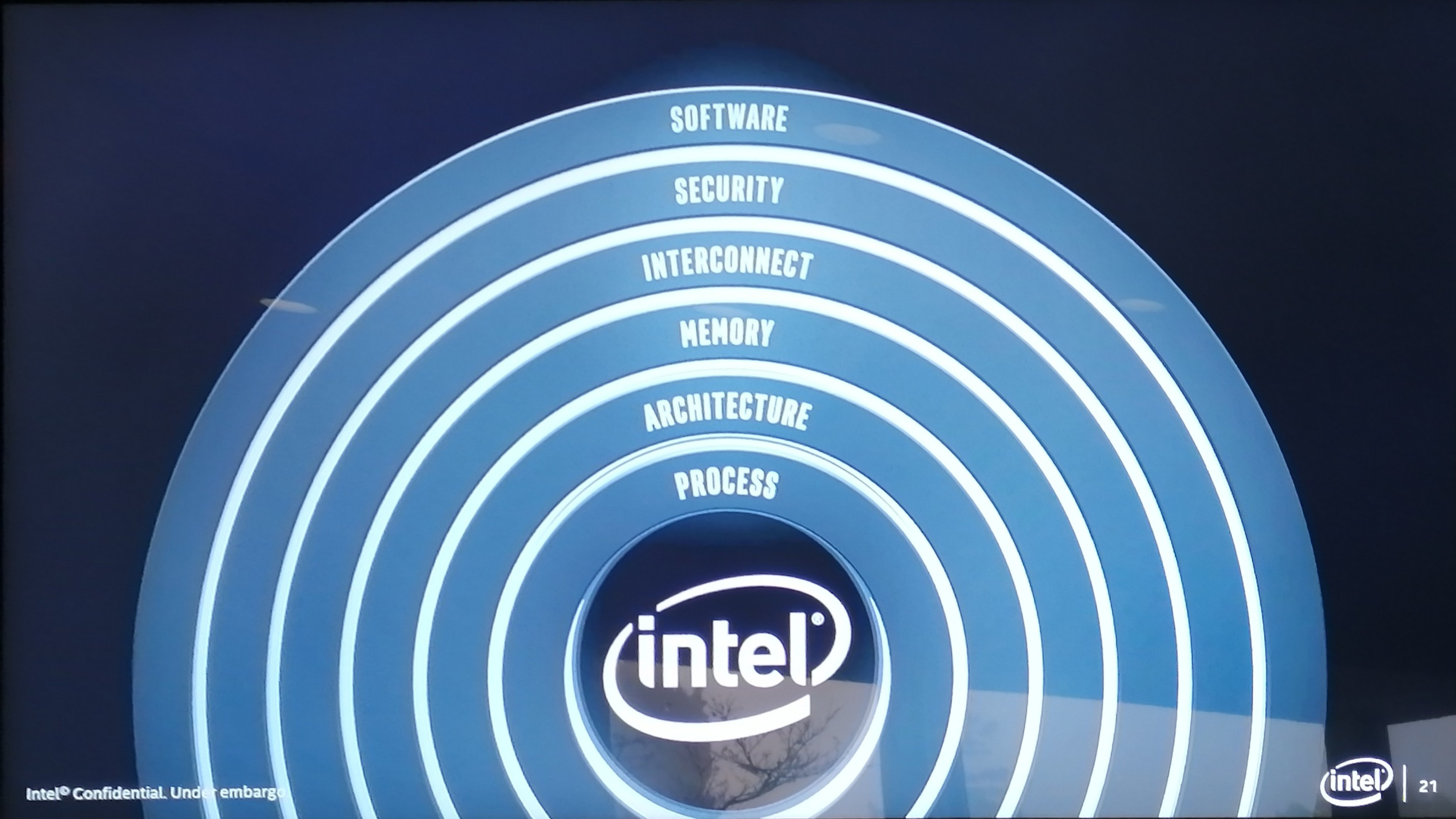
Through Intel’s Architecture Day, the company did a couple of side discussions for a few journalists to speak to Raja Koduri and Jim Keller in a round-table format. Beyond that, Murthy Renduchintala and Raja also held a Q&A session at the end of the day. They answered questions on 10nm, the new Foveros technology, Thunderbolt 3 adoption, and how Intel will approach 5G.
For this article, the Questions and Answers will be listed as an abridged version of the responses, due to time constraints and live transcription, with questions grouped based on topic. Different members of the press asked these questions.
 Raja Koduri |
 Jim Keller |
 Dr. Murthy Renduchintala |
| Chief Architect Senior VP Core and Visual Computing Group |
Senior VP Silicon Engineering Group |
Chief Engineering Officer Group President, Technology, Systems Architecture & Client Group |
Q: A lot of the CPU microarchitecture at Intel has been hamstrung by delays on process node technology. What went wrong, and what steps have been made to make sure it doesn't happen again?
R/J: Our products will be decoupled from our transistor capability. We have incredible IP at Intel, but it was all sitting in the 10nm process node. If we had had it on 14nm then we would have better performance on 14nm. We have a new method inside the company to decouple IP from the process technology. You must remember that customers buy the product, not a transistor family. It’s the same transformation AMD had to go through to change the design methodology when they were struggling. At Apple it was called the ‘bus’ method.
M: This is a function of how we as a company used to think about process node technologies. It was a frame tick (limiting factor) for how the company moved forward. We've learned a lot about how this worked with 14nm. We now have to make sure that our IP is not node-locked. The ability to have portability of IP across multiple nodes is great for contingency planning. We will continue to take aggressive risks in our designs, but we also will have contingency. We need to have as much of a seamless roadmap as possible in case those contingencies are needed, and need to make sure they are executed on ASAP if needed to keep the customer expectations in line. You will see future node technologies, such as 10/7, have much more overlap than before to keep the designs fluid. Our product portfolio on 14nm could have been much better if our product designs were not node-locked to 10nm.
R: In the future there will be no transistor left behind, no customer left behind, and no IP left behind.
Q: Will we ever see a 10nm monolithic desktop CPU at the high end?
R: Yes.
Q: How is 10nm? Has it changed?
R: It is changing, but it hasn't changed. There are a lot of lessons learned in how Intel approached it to begin with. We are established a much better model between manufacturing and design. We want good abstractions in product and process node going forward. When everything was going well, this issue didn't manifest and so wasn't an issue. There's complexity here when something bad happens on process, so the whole pipeline clogs up - the rest of the world solves this with abstraction. We need to make sure it won't happen again, and we have a desire to build resilience in the roadmap.
Q: Are there plans for mixed SoCs, combining CPU / GPU / AI / FPGA ?
R: In our roadmap there will be scalable vector/matrix combinations. What our customers want are very scalable solutions. Customers want similar programming models regardless of the silicon.
Q: What has been the effect of hiring Raja/Jim and bringing outsiders to Intel?
M: Intel is very innovative. We want to add to that chemistry and make sure we bring in people who understand Intel but also bring in good ideas. It's about respecting the rest of the market and make sure Intel is competitive. It's balancing the centre of internal debates by making sure we are challenging internal beliefs and the status quo by bringing in people who have done this sort of thing before. It shows to Intel's strengths in its ability to absorb interesting ideas from the outside. We went for the very best on the outside because that was what required to join with the very best on inside.
Q: What is Intel’s current approach to 5G, given the topics discussed today?
M: We think about 5G from the datacentre to the network to the edge and to the device. We at Intel believe the transition to 5G and its implications on the network, in terms of accelerating data and catalysing a software defined network where bespoke silicon gets replaced by containers, is as transformative as the jump from analogue to digital. It will accelerate the ‘cloudification’ of the network. The edge is important, especially to minimize latency for new services. Sub-millisecond latency for these services is critical. The over-the-air interface is important too. The intelligent cloud domain is going to be the flywheel about how fast the industry evolves. We mentioned in November that our XMM 5G modem will be in the hands of partners in the second half of 2019 with products in early 2020. It is a multi-mode 5G LTE architecture from day one, supporting all 3 mmWave bands, and sub-6 GHz frequencies.
Q: As Thunderbolt 3 requires additional chips, how do you see future OEM adoption?
M: Integrated Type-C Thunderbolt 3 is the first generation. We will refine it in the future - that's the natural genealogy of the technology. We constantly think about how much we integrate into the chip and how much we leave on the board.
R: This is a big IP challenge, not only for TB3, but for other IP. Integrated PHYs are important. For example, by disaggregating the transceiver in our FPGA line-up, it has allowed us to focus on that decoupled IP a lot.

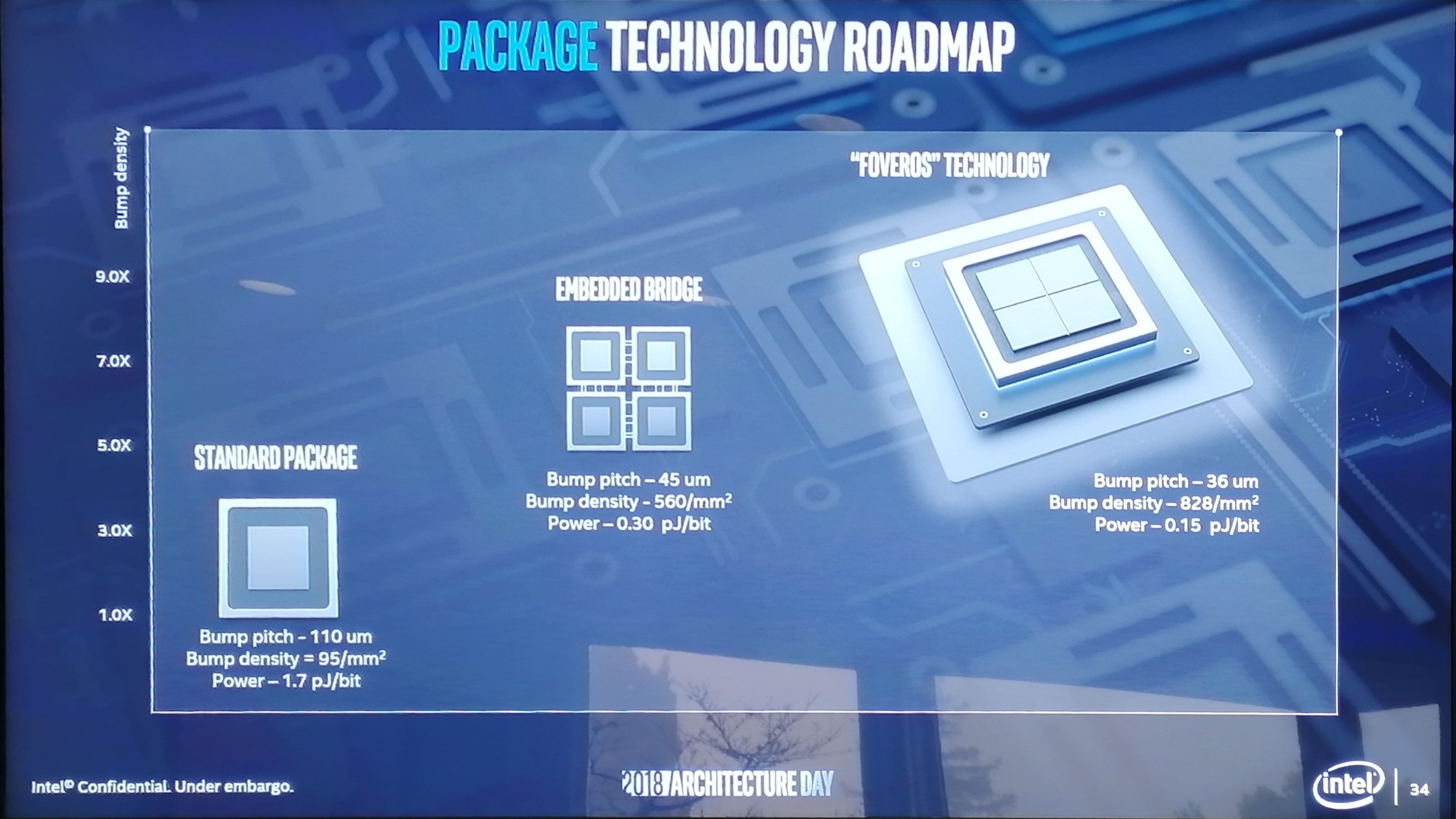
Q: In the demo of FOVEROS, the chip combined both big x86 cores built on the Core microarchitecture and the small x86 cores built on the Atom microarchitecture. Can we look forward to a future where the big and little cores have the same ISA?
R: We are working on that. Do they have to have the same ISA? Ronak and the team are looking at that. However I think our goal here is to keep the software as simple as possible for developers and customers. It's a challenge that our architects have taken up to ensure products like this enter the market smoothly. We’ll also have a packaging discussion next year on products like this. The chip you see today, while it was designed primarily for a particular customer to begin with, it’s not a custom product, and in that sense will be available to other OEMs.
M: We've made the first step on a journey. That first step is a leap, and the next step is incremental. As we've said about One API strategy – if we homogenise the API then it'll go into all our CPUs. FOVEROS is also a new part/product that shows that we had a gap in our portfolio – it has helped us create technologies to solve an issue and we expect to expand on this in the future with new IP.
Q: Are you having fun with FOVEROS?
J: Because Raja deals in GPUs, he’s having fun with high bandwidth communications between compute elements. It's a new technology and we're having some experimentation with it. What is frustrating is that as an industry we hit a limit for current flux density a year before stacking technology became viable, so for high performance on stacking we're trying a lot of things in different areas. There's no point having to make thermal setbacks if it also removes the reason why you're using the technology. But we're having fun and trying a lot, and we'll see FOVEROS in a number of parts over the next 5 years. We will find new solutions to problems we don't even know exist yet.
Q: When is Manufacturing Tech Day?
M: We will tell you when it happens! I'm sure you all have opinions on Intel 10nm right now and yes we are looking at what we're doing, eating an amount of humble pie, but we're re-adjusting our process to make sure that we can take the best process no matter what the product is.
The title of this page was a quote from Jim during the Q&A: 'At some point in the future you'll read an article with the title Intel Made Something Really Funny.'. I think I win this bet...


148 Comments
View All Comments
porcupineLTD - Thursday, December 13, 2018 - link
Can you articulate what you want to say with those links? or how they might contradict me/answer my question?ajc9988 - Thursday, December 13, 2018 - link
What I am saying with those links is that AMD has already evaluated the use of active interposers and is the company that is articulating a data protocol for active interposer routing so that it doesn't matter what each chiplet does on its own data routing, so that any chiplet could be attached to an active interposer and work. Further, in the 2017 white paper, it directly shows the reason that AMD hasn't yet adopted the active interposer is due to costs. Passive interposers can be used, but don't offer the benefit of active interposers. But, the cost of an active interposer is the same as doing a monolithic chip once the active interposer is produced on the 32nm or smaller active interposer. As such, adoption did not yet make sense until the costs are reduced.https://spectrum.ieee.org/tech-talk/semiconductors...
The earlier ones show AMD did research into the optimal topology for active interposers in 2014 and 2015. It shows the optimal core count for the benefit, latencies, etc.
Now, if you look at packaging solutions, say from GF, you find that 2.5D and 3D integration is only available on 32nm and 28nm processes, with 14nm coming soon. https://www.globalfoundries.com/sites/default/file...
I bring up GF doing the packaging as, due to the WSA, even if they cost more than competitors, being able to potentially count the wafers used for the active interposers against the WSA would reduce the fines payed under that contract for doing fabrication at TSMC, making it potentially, on net, cheaper.
Now, there is an article today from Anand saying Intel is releasing the B365 chipset on 22nm. ( https://www.anandtech.com/show/13714/intel-adds-b3... ) Intel was forced to move chipsets back to 22nm due to the 10nm process not being ready for mass deployment which caused a shortage of 14nm capacity. This means Intel could not shut down their 22nm fabs to cut that capacity. As such, a fab needs to stay as close to capacity as possible or else it bleeds money (hence why AMD eventually went fabless). So, Intel using 22nm fabs to do the 22nm active interposer is just Intel making lemonade on tech that few others adopted in the industry yet due to the basis of costs. If you go back to the cost study AMD did, the active interposer at 20nm is around the cost of doing a monolithic die, which is what Intel has done to date. So it isn't really costing them more to add in the active interposer at all, while saving expenditures by keeping the 22nm fabs full of jobs, while having awesome yields on the active interposers due to it being a very mature node with low defect rates, etc. If you examine the amount of area AMD estimated is needed for the logic routers, you can see only 1%-10% area on the active interposer is needed to achieve the goal, meaning the chances a critical defect hits the active interposer is very low.
But, as to it making AMD do it, that is the wrong thinking. AMD already plans to adopt it, just not until the costs of doing so are lower. They will check the IC Knowledge lists to see when costs make sense.
But, if you look at all that data I provided, AMD has all the solutions to the problems encountered with using an active interposer. All they are waiting for is it to be cost effective. Intel isn't leading anything here, other than doing it because they need to justify and subsidize having to keep certain 22nm fabs open because of their chipsets due to the delays in 10nm. Doesn't take a genius to figure it out, just takes someone paying attention to the tea leaves.
ajc9988 - Thursday, December 13, 2018 - link
Also, I forgot to mention that the 2.5D integration of HBM Phy onto a stitched interposer was accomplished last year. This suggests that HBM could be added to an active interposer when AMD eventually does adopt an active interposer. Meanwhile, with only 1-10% of the active interposer being used according to their papers, it leaves room for in the future having elements of the I/O chip being moved to the active interposer as an additional way that things easily could develop. The question is what benefit it would be to produce what on the 32nm or 28nm nodes over having their I/O disintegrated die on 14nm. But I would bet AMD has an idea of what would be better where and will consider it when eventually adopting, considered the detailed paper on routing topology of active interposers in that group of links.porcupineLTD - Thursday, December 13, 2018 - link
Thank you for the detailed response its very informative however its besides my comment, IF Intel ships its chiplet on interposer design in 2019 they will be first (regardless of the reasons or economics behind it), as for AMD not doing it now it's again besides my comment, I wandered if they will do this for ZEN 3 or 4 not ZEN2, ZEN 3 will launch in 2020 when (as far as I know) the WSA expires so what GF does or doesn't do is not that relevant (I would be curious to know about tsmc's or samsung's packaging/interposer offerings). The result (if they implement it in ZEN3/4) will come down to cost (as you point out), socket compatibility (can it be done on the current server socket?) and planning (ZEN3 design is almost done right now so even if the interposer cost is down AMD can't implement it if they didn't predict this one year ago).porcupineLTD - Thursday, December 13, 2018 - link
Also Anandtech, I am not versed in web design, but is it really that hard to have a comment section that doesn't utterly suck? Is it really that hard to introduce an edit function, or at least a delete one?(an upvote/donvote system would be asking for too much).ajc9988 - Thursday, December 13, 2018 - link
Forgive me, many think that Intel is showing through using it that they are significantly ahead in the field of active interposers and 2.5D and 3D chiplet integration, meaning that it would take years for other chip designers to catch up, which isn't the case. So I do apologize for that assumption in regards to you.What those do show is AMD does have plans to do so in the future, it is just a matter of timing. On the socket part, there is a chance they are introducing a new socket in order to support PCIe 4.0 on the upcoming Zen 2 chips, which comes from analyzing their wording from the Next Horizon event on Nov. 6th. Meanwhile, we know that PCIe 5.0 will be finalized potentially in the first half of next year and AMD did mention DDR5 potentially being available for Epyc 3 chips based on Zen 3, but that mainstream chips will not support DDR5 in 2020 (leaves open that TR HEDT platforms may or may not get DDR5 support at that time). Intel has not provided information on when PCIe 4.0, 5.0, or DDR5 will be supported. As such, though, AMD may have backwards compatibility on the CPUs for socket compatibility, but may require a new socket for the new boards containing the new features, which I think is understandable to many in the server and workstation spheres. It is also the reason I may wait for 2020 to upgrade my 1950X rather than next year (if you are going to buy a new board, and there is a chance that board won't contain the new feature sets that release that year, waiting one more year is fine IF your workloads won't suffer for the wait).
But, I read somewhere Intel hinted at 1GB of RAM being integrated with the active interposer processors, acting as an L4 cache. Although not novel (those articles I gave for AMD whitepapers from 2014 and 2015 specifically dealt with on package integration of memory and latencies involved, suggesting we could see some type of 3d memory solution integrated when AMD does incorporate an active interposer), seeing the latencies involved with Crystalwell, which was the eDRAM on Broadwell, suggests that Intel will get a significant uplift in certain workloads, as well as keeping the chip primed and having to go off chip less often for memory calls, which is fantastic. Intel also kept the power delivery part under wraps, which is something that does excite me, but we were given no information about it (possibly bringing FIVR back, which was rumored for Ice and Tiger lake anyways).
Also, on compatibility, part of the reason I gave the article discussing data protocols for active interposers is that the routing is chiplet agnostic, meaning you can integrate parts that have their own internal routing and not effect it. Then just comes down to appropriate socket wiring, which I mentioned they may need new sockets for these features, while just maintaining drop in compatibility for consumer side.
Here is some information on other packaging types out there in the market. I am including them, but as this is just being researched, I am not attesting veracity or relevance, fully. I will have glanced through them, but you understand.
http://s3.amazonaws.com/sdieee/1817-SanDiegoCPMTDL...
"DIGITIMES reports that the new TSMC plant in Chunan will be dedicated to offering the foundry’s in-house developed advanced packaging technologies: CoWoS (chip-on-wafer-on-substrate) and integrated fan-out (InFO) wafer-level packaging, and its newly-unveiled system-on-integrated-chips (SoIC) and wafer-on-wafer (WoW) packaging services."
https://criticalmaterials.org/tsmc-to-set-up-new-f...
https://fudzilla.com/news/pc-hardware/47265-tsmc-t...
https://electroiq.com/2018/10/synopsys-design-plat...
Older article for foundational work from 2014:
https://semiengineering.com/time-to-revisit-2-5d-a...
2016 follow up: https://semiengineering.com/2-5d-becomes-real/
Packaging Market from February 2018:
http://worldherald24.com/2018/02/19/global-3d-ic-a...
Paper and slide show discussing the implementation and challenges of 3D packaging from 2016:
https://smtnet.com/library/files/upload/25d-3d-sem...
Sorry for the data dump at the end. I do apologize about that.
tommybobberson - Saturday, December 15, 2018 - link
just clarifying, do you mean to use such methods, amd would need to rive up production costs which reduces their profit/value. but since intel already has a high production cost, such methods would not affect them?ajc9988 - Wednesday, December 19, 2018 - link
tommybobberson - in a manner of speaking, yes. How much it costs to produce effects margins and pricing. One reason AMD could price the high core chips in such a manner, aside from effective yields for products, is the decreased costs to produce high core count products. If AMD added the active interposer now, it would rise production costs to be the same as a monolithic die, which would then require either an increase in market price of the products or a decrease in margins for their products.Intel, on the other hand, never captured the extra margin of going to chiplets before introducing the stacked chips. That means that the active interposer cost to them is less as the price to do so matches the cost of a monolithic die. As such, Intel can maintain their current pricing while introducing the stacked die on active interposer. Further, due to filling up 22nm fab time (because of 10nm causing a shortage of 14nm fab time which required Intel to move certain lines back to 22nm, likely forcing some plants planned to be closed or retrofitted to remain on 22nm), Intel will be able to help on the cost of 10nm delay, thereby mitigating some of the effects found in not having 10nm up and running by now.
Supercell99 - Friday, December 14, 2018 - link
With all the hackers, PC gaming is dying.sgeocla - Wednesday, December 12, 2018 - link
Fist they mock your chiplets by saying you glue your dies together, then they fail to compete with you and then years after they copy your chiplets and call it revolutionary.This is why Intel can no longer have public presentations of their own failures and have to have privately controlled presentations.