Intel's Architecture Day 2018: The Future of Core, Intel GPUs, 10nm, and Hybrid x86
by Dr. Ian Cutress on December 12, 2018 9:00 AM EST- Posted in
- CPUs
- Memory
- Intel
- GPUs
- DRAM
- Architecture
- Microarchitecture
- Xe
Changing How Chips are Made: 3D Packaging with FOVEROS
Anyone who has followed any amount of chip design in semiconductors should well-aware that most of the CPUs and SoCs in production today are based on monolithic dies – single pieces of silicon the have all what is needed inside, before being placed on a package and into a system. While rarer, there are multi-chip packages, were multiple chips go in one package with a shared connection. Beyond this we have seen interposers or embedded bridges designed to bring different chips together with high-speed interconnects. Now Intel is ready to bring 3D stacking into the mass market.
One of the biggest challenges in modern chip design is minimizing die area. A small die decreases costs – typically power too – and can make it easier to implement in a system. When it comes down to extracting performance however, we are at the limits of scale – one of the downsides of big monolithic dies, or even multi-chip packages, is that memory is too far away. Intel today is now ready to talk about its Foveros technology, which involves active interposers in small form factors to bring differentiated technologies together.
Foveros: It’s Greek for Awesome, Apparently
The way Raja introduced this technology started with discussing process technologies. Intel has for many years/decades been focused on high performance process nodes, trying to extract as much as possible from its high-performance cores. Alongside this, Intel also runs an IO optimized process node on a similar cadence but more suitable for PCH or SoC-type functions.
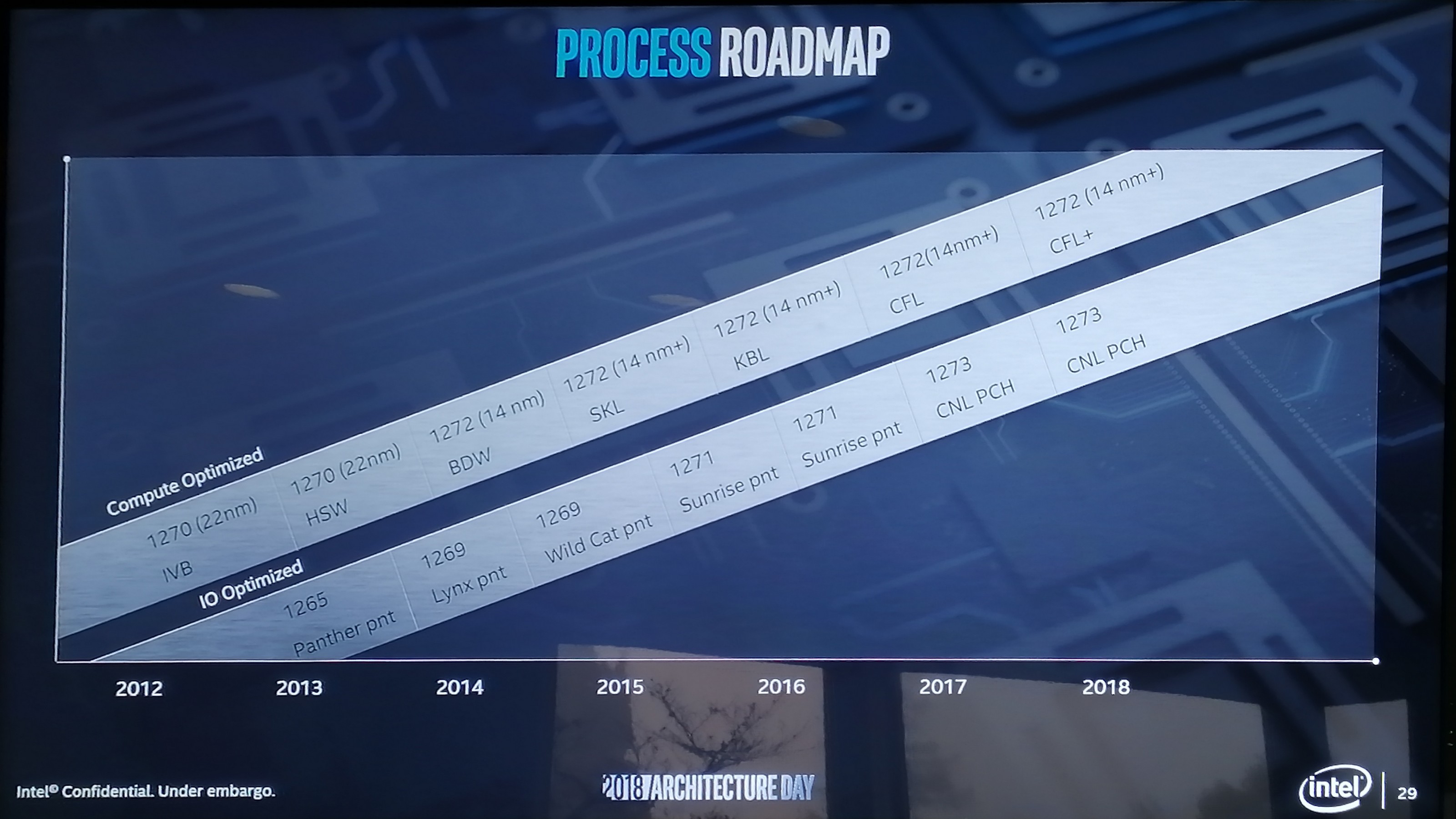
The 126x and 127x are the internal numbering systems for Intel’s process node technologies, although they don’t differentiate between BKM updates for the "+" node variants it turns out. But the point here is that Intel already knows that it needs certain process optimizations in place depending on the type of transistors, performance, and power needed. Going forward, Intel is going to be expanding its node base out so it can cover more power and performance points.
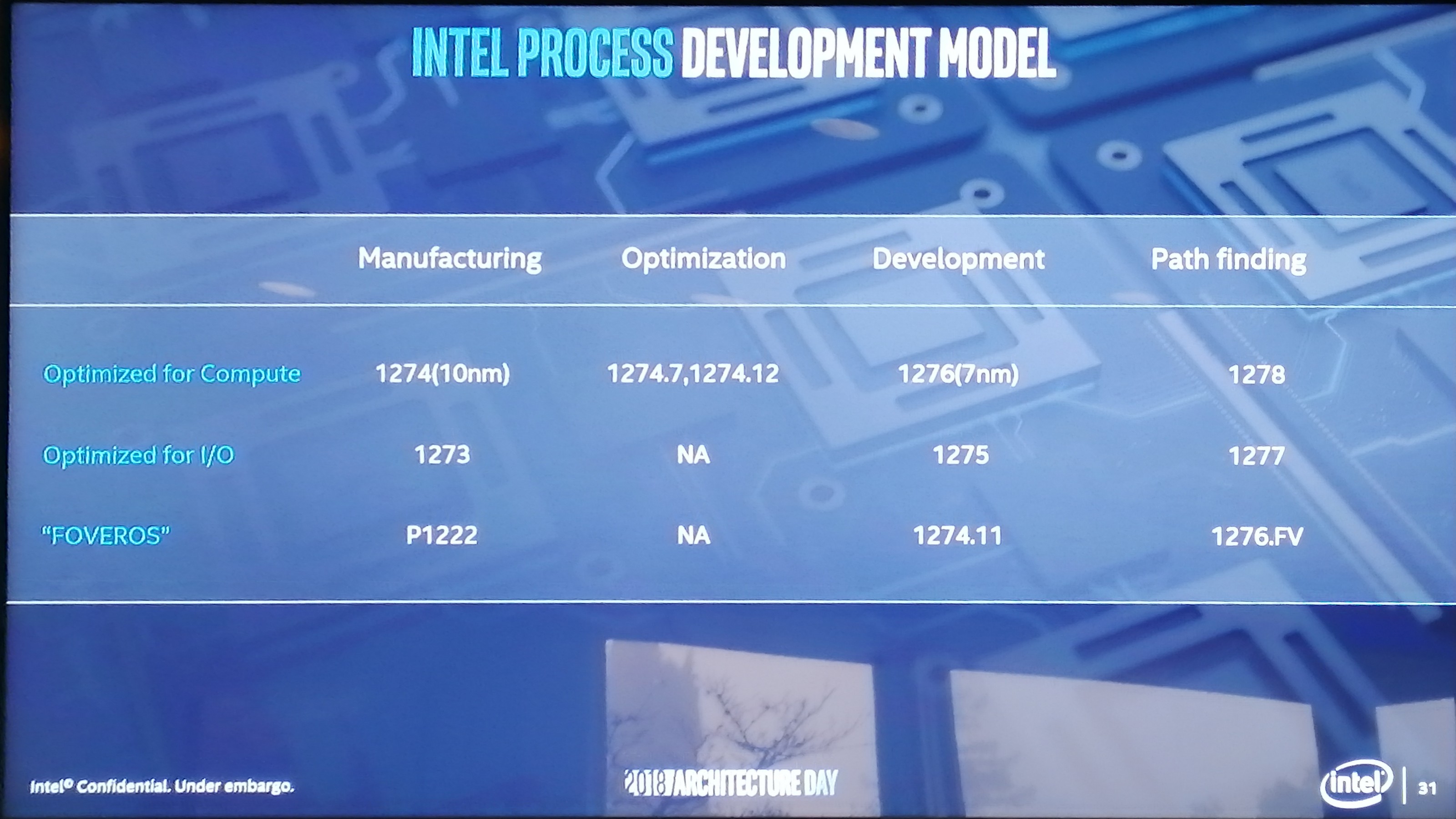
So for this example, Raja pulled out the current set of process technologies for 2019. For a manufacturing process, compute has the 1274 process on 10nm, IO has the 1273 process (14nm), while this new special Foveros technology is under P1222. Alongside the manufacturing, Intel will be working on optimizations focusing on the compute aspects of the manufacturing node. There will also be a set of developments for future node technologies, and the final column shows that Intel has path-finding research to look into future technologies and determine what capabilities will be possible on future designs. This sounds pretty much what a company like Intel should be doing, so no argument from me so far. The goal here is that each type of transistor use case can be different, and there isn’t a one-size fits all approach.

One way to assist with this is through chiplets and packaging. By picking the best transistor for the job in each case, whether it is CPU, GPU, IO, FPGA, RF, or anything else, with the correct packaging, it can be put together to get the best optimizations available.
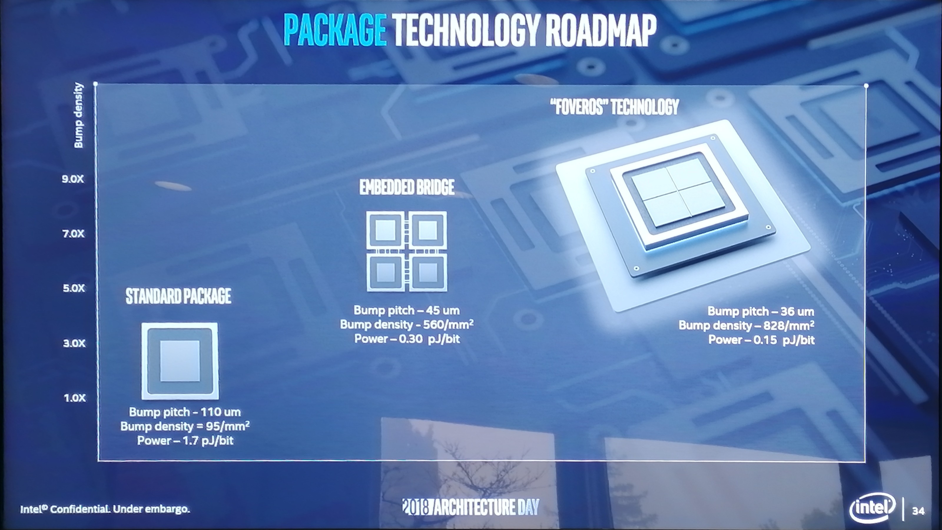
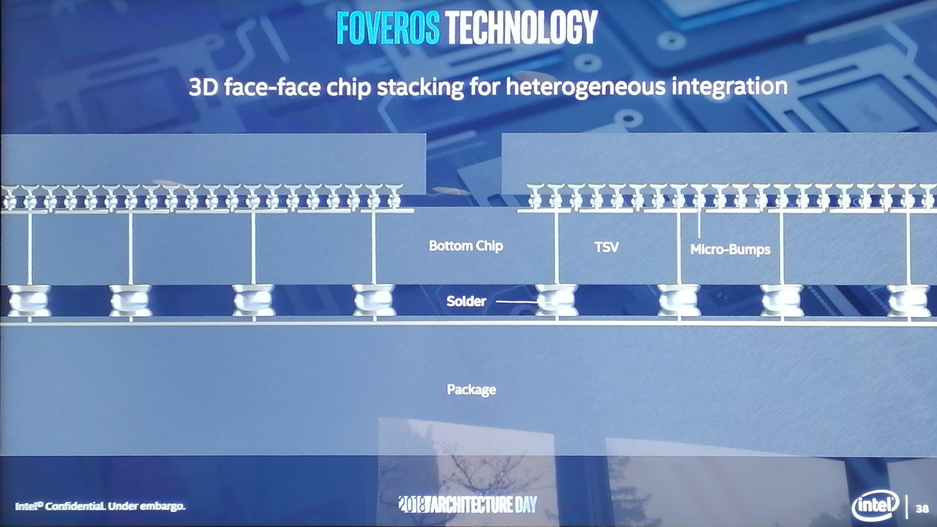
So here’s where Foveros fits in. Foveros is Intel’s new active interposer technology designed as a step above its own EMIB designs for small form-factor implementations, or those with extreme memory bandwidth requirements. For these designs the power per bit of data transferred is super low, however the packaging technology has to deal with the decreased bump pitch, the increased bump density, and also the chip stacking technology. Intel says that Foveros is ready for prime time, and they can produce it at scale.
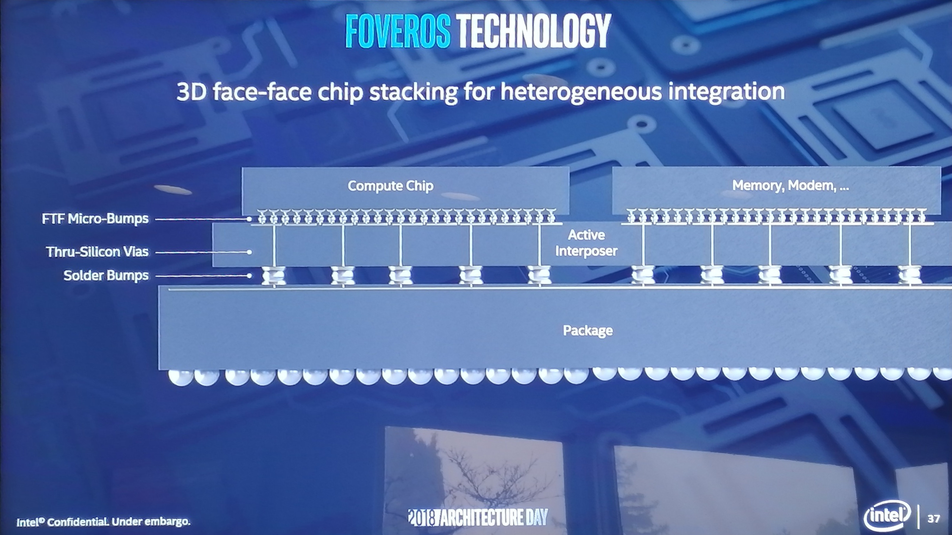
So this Foveros ‘3D’ packaging just sounds like a silicon interposer, such as what we’ve seen on AMD’s Fiji or NVIDIA’s high-end datacenter GPUs. However Intel is going above what those products are doing by actually making the interposer part of the design. The interposer contains the through-silicon vias and traces required to bring power and data to the chips on top, but the interposer also carries the PCH or IO of the platform. It is, in effect, a fully working PCH, but with vias to allow chips to be connected on top.
The first iteration of this technology is less complicated that the slide above, just using a set of CPU cores attached to the PCH below, but the idea is that a large interposer can have select functions on it and those can be removed from the chips above to save space. This also lets Intel use the different transistor types in different chips – the example we were given uses an interposer built on the 22FFL process node, with a 10nm set of CPUs on the top die. Above this, DRAM is provided in a POP package. Sounds cool, right?
In actual fact, Intel had a Foveros chip or two working in the demo area. These, Intel explained, were hybrid x86 designs that combined a single big Core with four smaller Atom cores on the same 10nm piece of silicon. I’m sure I’ve heard about big.Little before, but I was shocked that Intel is actually going to do it! We managed to take a photo of the block diagram, which Intel removed from its slide deck before sending it out to the press after the presentations. All details on the next page.


148 Comments
View All Comments
ajc9988 - Thursday, December 13, 2018 - link
https://www.anandtech.com/show/13445/tsmc-first-7n...Risk production is in Q2 next year. And Mass is listed by Q2 2020 for 5nm.
https://www.extremetech.com/mobile/278800-tsmc-exp...
So, I was a bit off by the estimate for volume being 2020, but you were off on when risk production starts. Meanwhile, 7nm+ is already confirmed for AMD on Zen3, as the benefits of 5nm+ don't outweigh the costs associated moving to the process for AMD. This is why it is thought AMD will skip 5nm and try 3nm when available. But, TSMC has not said when 3nm will be available, while Samsung is saying 3nm in 2021:
https://semiengineering.com/big-trouble-at-3nm/
https://www.cdrinfo.com/d7/content/samsung-details...
http://www.semimedia.cc/?p=2524 (saying TSMC 3nm in 2022/23)
I cannot find the article speculating Apple will be the first customer on 5nm EUV and when ATM.
HStewart - Thursday, December 13, 2018 - link
"Nodes are marketing jargon"Exactly - it reminds me the frequence wars back in P4 days. But if you look closely at Intel's plan - I am no chip designer - even though I did take Micro-code Enginnering classes in College, but Foveros is revolutionary design - I thought EMiB was amazing, but to do that in 3rd diminsion is awesome - maybe one they could even stack cores that way - instead huge chip monsters.
But a nm rating by vendor 1 does not nm rating by vendor 2 - what underneath makes the different - Intel is extremely smart to decouple nm process from actual archexture. If you notice by Intel archiexture Intel has more improvements in core archiexture over next 3 years - this is because they are not limited by process (nm)
ajc9988 - Friday, December 14, 2018 - link
EMIB was not revolutionary and neither is foveros. They are incremental steps and existing competing solutions are available and have been for some time. Not only that, it will only be used on select products with eventual spread to the stack.Go to the second page of comments and see my links there. I think you will find those quite interesting. Not only that, this has been done with HBM for years now. If you look at AMD's research, almost half a decade ago, they were studying optimal topologies for active interposers. They found only 1-10% of the area was needed for the logic routing of an active interposer. Moving a couple I/O items onto the active interposer just is an extension. In fact, you can put those components on a spread out interposer between the above chiplets that sit on the interposer, but would need to plan on the heat dissipation or having so low a heat that it doesn't need sinked.
Considering lack of details of what is on the active interposer or timeline for mainstream, HEDT, and server markets, I will assume those won't see this until 2020, with the first products being mobile in nature.
In fact, Intel this summer gave AIB patents to DARPA to try to control what tech is used for chiplets moving forward, proposing that be used. AMD proposed a routing logic protocol which would be agnostic to routing on the chiplets itself, increasing compatibility moving forward.
Now, if EMIB is so "revolutionary", do the Intel with AMD GPUs seem revolutionary? Because that is the only product that comes to mind that uses it. Those chips are Hyades Canyon and Crimson Canyon. It isn't that dissimilar to other data fabric uses.
So far, on disintegration of chip components, AMD's Epyc 2 is getting there. It literally uses just cores and the interconnect for the chiplet (for this description, I am including cache with the cores, but when latency is reduced with active interposers, I do expect an L3 or L4 or higher caches or integrated memory on package to be introduced external to the "core" chiplet moving forward). From there, we could see the I/O elements further subdivided, we could see GPU, modems, etc. But all of this has been planned since the 2000s, so I don't see anything new other than the culmination around the same time other alternative solutions are being offered, just that the cost/benefit analysis has not tipped in its favor just yet, but should in the next year or so, which should bring many more designs to the forefront. Here is a presentation slideshow discussing the state of current 2.5D and 3D packaging. After review, I'd like to hear if you still think EMIB and Foveros are "revolutionary." Don't get me wrong, they are an incremental success and should be honored as such. But revolutionary is too strong a word for incremental process. Overall, it changes nothing and is the culmination of a lot of work over a decade by numerous companies and engineers. Even competing solutions can act as inspiration for another company moving forward and Intel's engineers read the whitepapers and published peer reviewed articles on the cutting edge, just like everyone else in the industry.
As to you saying Intel is smart to do it, they haven't done it except in silicon in labs and in papers, unless talking the EMIB with Intel CPU. AMD has a product line, Epyc 2, where the I/O is made at GF on 14nm and the chiplet is made on 7nm TSMC with greater pitch disparity. Intel hasn't really removed the components off the core chip yet into each separate element. ARM is considering something similar, and this is the logical progression for the custom designed chips for RISC V moving forward (may take a little longer, less well funded).
Meanwhile, this doesn't seem to stack high performance cores on high performance cores. The problem of thermals cooking the chip are too great to solve at this moment, which is why low power components are being placed relative to the higher performance (read as higher heat producing) components. Nothing wrong with that, it makes sense.
But, what doesn't make sense is your flowering lavish praise on Intel for something that doesn't seem all that extraordinary in light of the industry as a whole.
johannesburgel - Thursday, December 13, 2018 - link
People keep saying the same thing about Intel's 14nm process, which is allegedly equal or better than other fab's 10nm processes. But AMD currently makes products on 14nm and 12 nm processes which Intel apparently can't build on its own 14nm process. For example there is still no 32-core Xeon while AMD will soon ship 64 core EPYCs and lots of other companies have 32/48/64 core designs on the market. Many Intel CPUs have much higher effective TDPs than their equivalent AMD CPUs.So pardon me if I am not willing to simply believe in all this "Intel's process is better in the end" talk.
HStewart - Thursday, December 13, 2018 - link
But intel's single core performance is better than AMD's single core performance. Just because AMD glues 8 core cpus together does not make them betterIcehawk - Thursday, December 13, 2018 - link
Node isn't even close to everything.Rudde - Wednesday, December 12, 2018 - link
Gen 11 graphics in desktops is said to reach double the performance of gen 9.5 desktop graphics. 2W Atoms have half the max frequency of desktop graphics and half or three quarters of the execution units. The 7W custom hybrid processor has the full amount of execution units. I'd guess it has half the frequency of it's desktop counterpart to stay within power limits. This would put it at the same performance as 9.5-gen desktop parts, or actually at 30% higher performance.Think about that. 80% single thread performance compared to current high-end desktop processors (my quick est.) and 130% graphics performance. That's a solid notebook for web browsing, legacy programs and even for light gaming. All that at a power budget of a tablet.
If I were to bet, I'd bet on a MS Surface Book.
Spunjji - Thursday, December 13, 2018 - link
Now that would be nice!Intel999 - Wednesday, December 12, 2018 - link
Keep in mind that 3DXpoint came to market three years past the initial promise from Intel. 10nm will be appearing 4 or 5 years late depending on when volume production materializes.Chances are that this 3D stacked promise for late 2019 will show up around 2022.
I'm seeing alot of fellow Intel fanboys show a semblance of confidence that has been absent in recent months and rightfully so.
Let's all hope Intel can deliver this time on time.
ajc9988 - Wednesday, December 12, 2018 - link
I disagree on worrying about Intel with the active interposer. They use passive interposers for the mesh on HEDT and Xeons and Xeon Phi (since around 2014) for years now. The 22nm active interposer is to fill out fab time due to pushing chipsets back to plants that were going to be shut down due to moving to 10nm, which never came.Meanwhile, AMD did a 2017 cost analysis saying that below 32nm would cost as much as a monolithic die, so it seems they are waiting due to cost, not on technical capability.
Either way, Intel doesn't hit 7nm until 2021, around the time 3nm may be ready at TSMC, if they go to 3nm within a year of volume 5nm products expected in 2020. That means Intel will never regain the process lead moving forward in any significant way, unless everyone else gets stuck on cobalt integration.