Intel's Architecture Day 2018: The Future of Core, Intel GPUs, 10nm, and Hybrid x86
by Dr. Ian Cutress on December 12, 2018 9:00 AM EST- Posted in
- CPUs
- Memory
- Intel
- GPUs
- DRAM
- Architecture
- Microarchitecture
- Xe
Changing How Chips are Made: 3D Packaging with FOVEROS
Anyone who has followed any amount of chip design in semiconductors should well-aware that most of the CPUs and SoCs in production today are based on monolithic dies – single pieces of silicon the have all what is needed inside, before being placed on a package and into a system. While rarer, there are multi-chip packages, were multiple chips go in one package with a shared connection. Beyond this we have seen interposers or embedded bridges designed to bring different chips together with high-speed interconnects. Now Intel is ready to bring 3D stacking into the mass market.
One of the biggest challenges in modern chip design is minimizing die area. A small die decreases costs – typically power too – and can make it easier to implement in a system. When it comes down to extracting performance however, we are at the limits of scale – one of the downsides of big monolithic dies, or even multi-chip packages, is that memory is too far away. Intel today is now ready to talk about its Foveros technology, which involves active interposers in small form factors to bring differentiated technologies together.
Foveros: It’s Greek for Awesome, Apparently
The way Raja introduced this technology started with discussing process technologies. Intel has for many years/decades been focused on high performance process nodes, trying to extract as much as possible from its high-performance cores. Alongside this, Intel also runs an IO optimized process node on a similar cadence but more suitable for PCH or SoC-type functions.
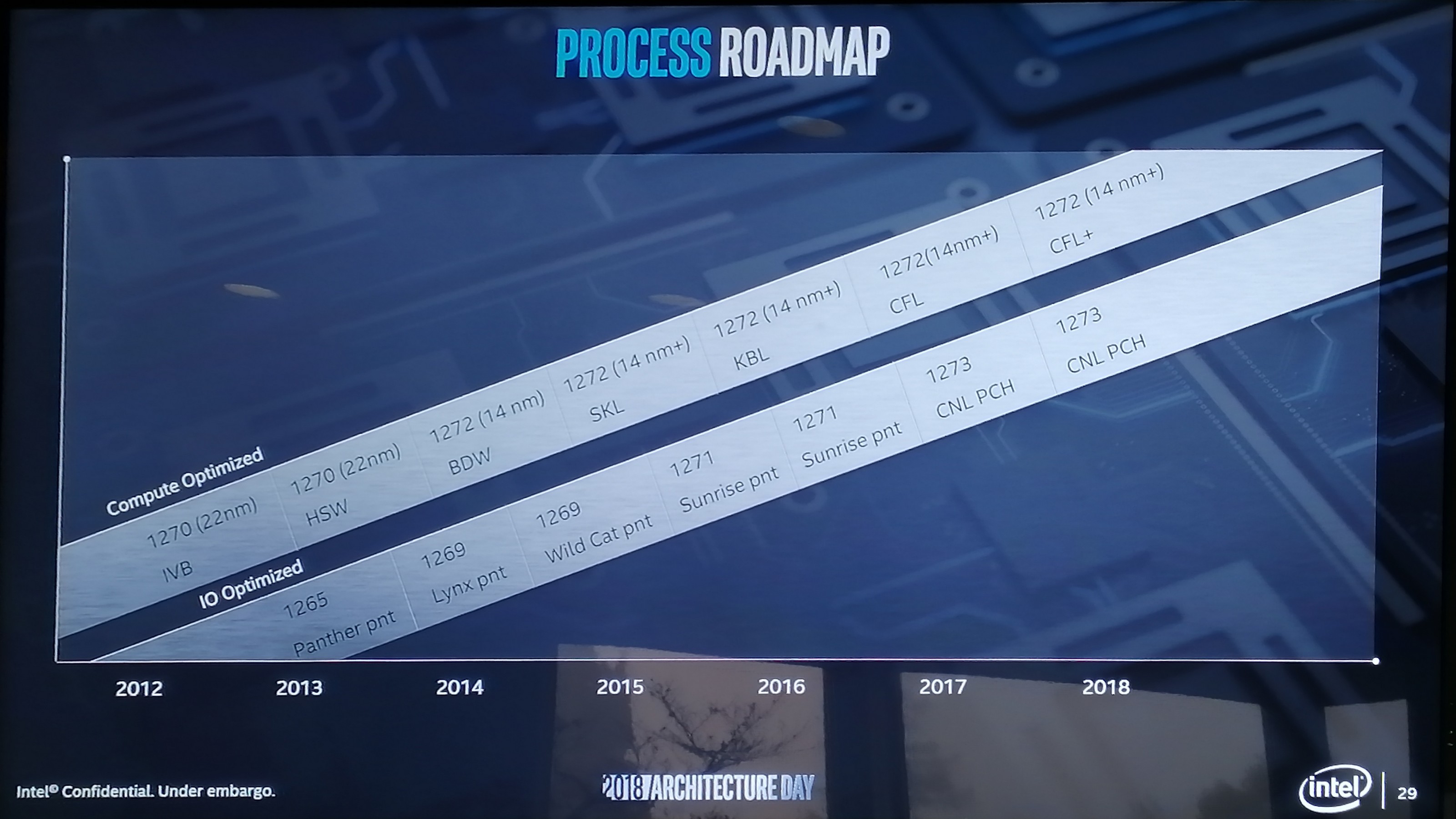
The 126x and 127x are the internal numbering systems for Intel’s process node technologies, although they don’t differentiate between BKM updates for the "+" node variants it turns out. But the point here is that Intel already knows that it needs certain process optimizations in place depending on the type of transistors, performance, and power needed. Going forward, Intel is going to be expanding its node base out so it can cover more power and performance points.
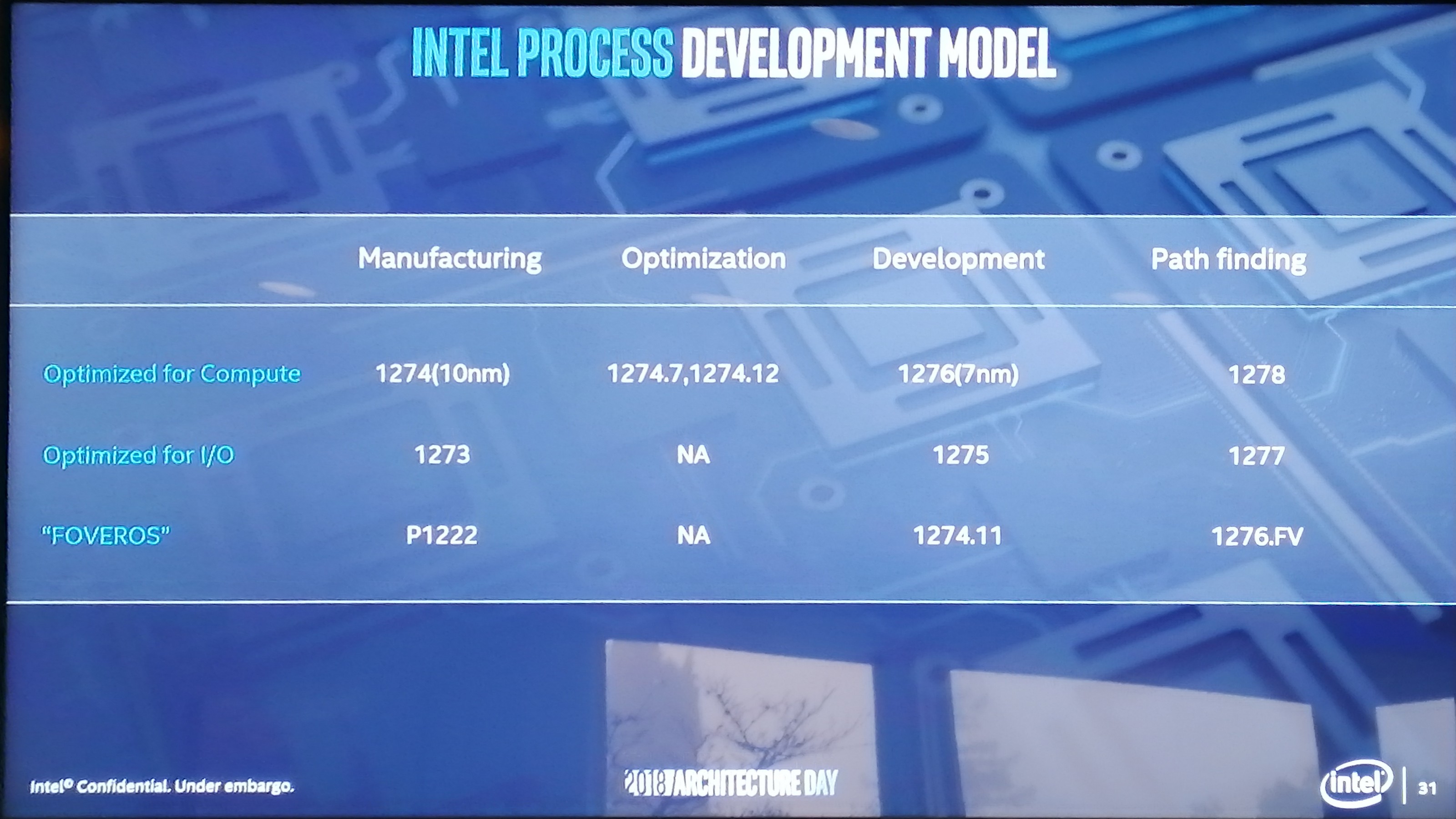
So for this example, Raja pulled out the current set of process technologies for 2019. For a manufacturing process, compute has the 1274 process on 10nm, IO has the 1273 process (14nm), while this new special Foveros technology is under P1222. Alongside the manufacturing, Intel will be working on optimizations focusing on the compute aspects of the manufacturing node. There will also be a set of developments for future node technologies, and the final column shows that Intel has path-finding research to look into future technologies and determine what capabilities will be possible on future designs. This sounds pretty much what a company like Intel should be doing, so no argument from me so far. The goal here is that each type of transistor use case can be different, and there isn’t a one-size fits all approach.

One way to assist with this is through chiplets and packaging. By picking the best transistor for the job in each case, whether it is CPU, GPU, IO, FPGA, RF, or anything else, with the correct packaging, it can be put together to get the best optimizations available.
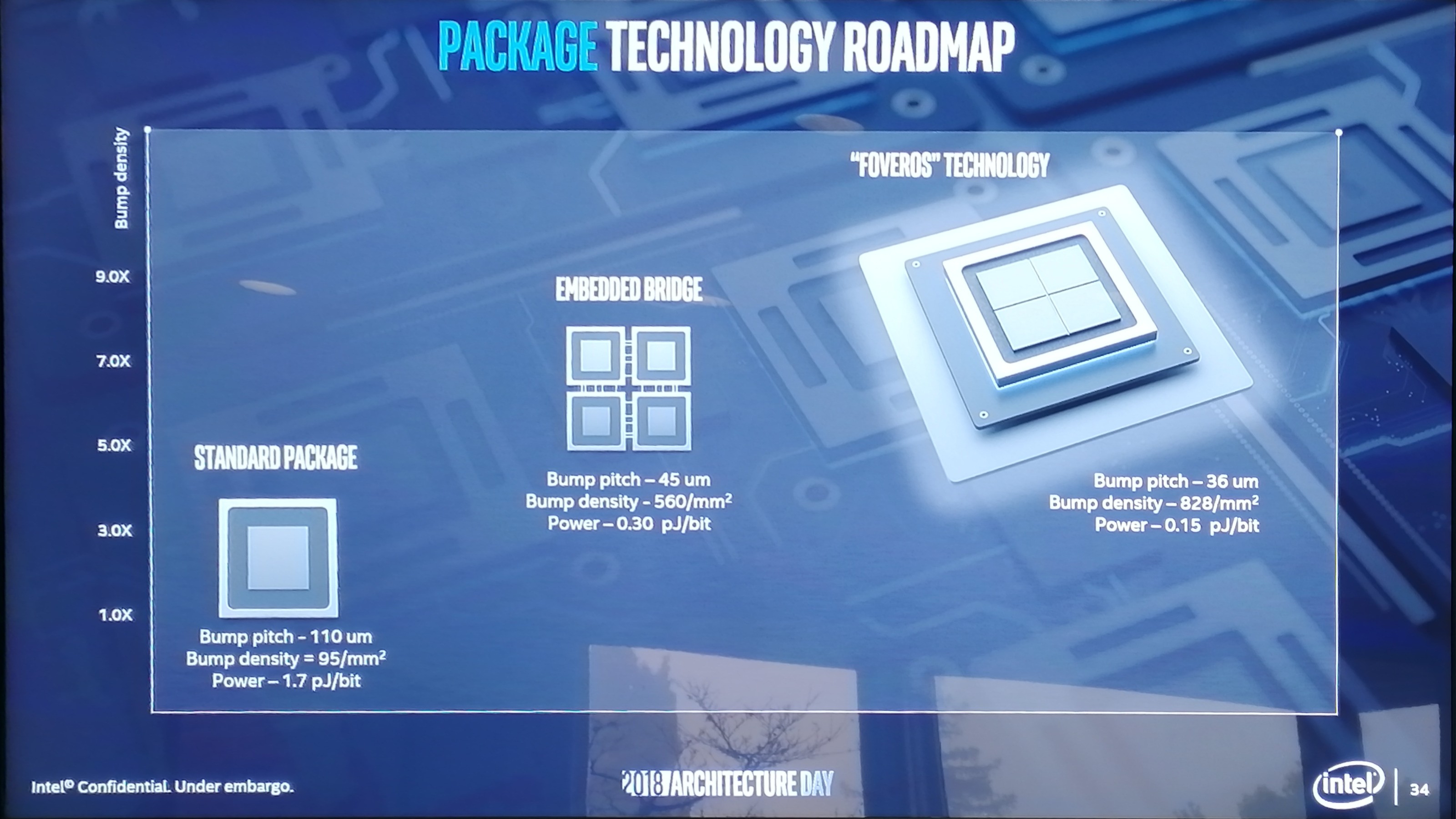
So here’s where Foveros fits in. Foveros is Intel’s new active interposer technology designed as a step above its own EMIB designs for small form-factor implementations, or those with extreme memory bandwidth requirements. For these designs the power per bit of data transferred is super low, however the packaging technology has to deal with the decreased bump pitch, the increased bump density, and also the chip stacking technology. Intel says that Foveros is ready for prime time, and they can produce it at scale.
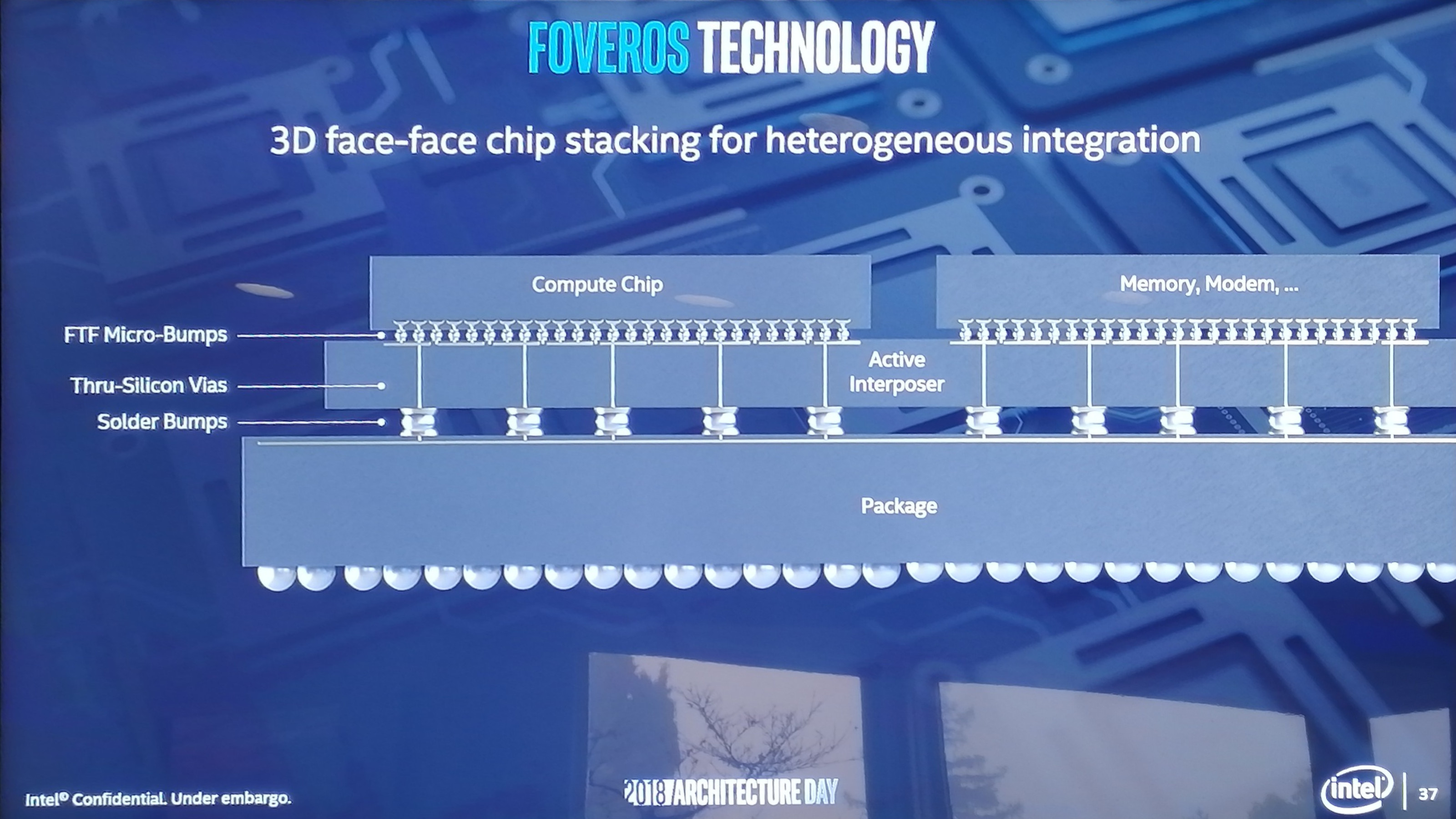
So this Foveros ‘3D’ packaging just sounds like a silicon interposer, such as what we’ve seen on AMD’s Fiji or NVIDIA’s high-end datacenter GPUs. However Intel is going above what those products are doing by actually making the interposer part of the design. The interposer contains the through-silicon vias and traces required to bring power and data to the chips on top, but the interposer also carries the PCH or IO of the platform. It is, in effect, a fully working PCH, but with vias to allow chips to be connected on top.
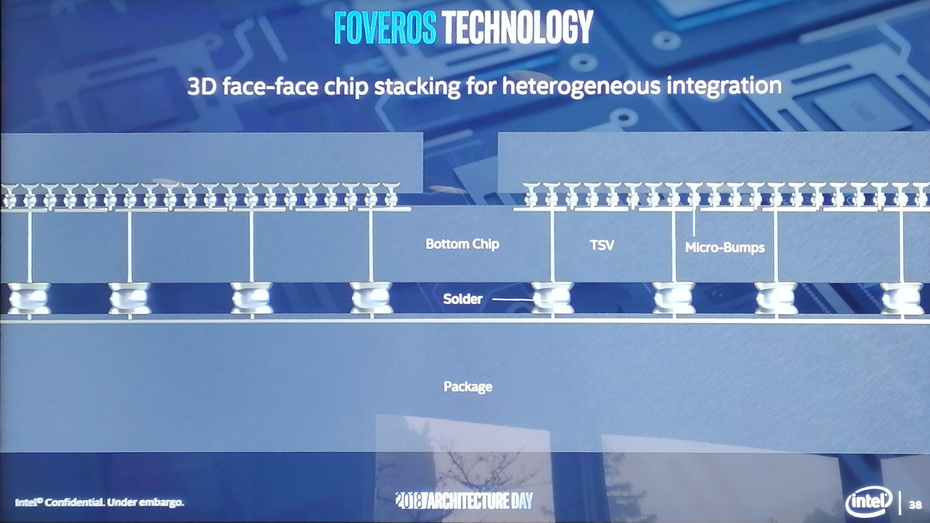
The first iteration of this technology is less complicated that the slide above, just using a set of CPU cores attached to the PCH below, but the idea is that a large interposer can have select functions on it and those can be removed from the chips above to save space. This also lets Intel use the different transistor types in different chips – the example we were given uses an interposer built on the 22FFL process node, with a 10nm set of CPUs on the top die. Above this, DRAM is provided in a POP package. Sounds cool, right?
In actual fact, Intel had a Foveros chip or two working in the demo area. These, Intel explained, were hybrid x86 designs that combined a single big Core with four smaller Atom cores on the same 10nm piece of silicon. I’m sure I’ve heard about big.Little before, but I was shocked that Intel is actually going to do it! We managed to take a photo of the block diagram, which Intel removed from its slide deck before sending it out to the press after the presentations. All details on the next page.


148 Comments
View All Comments
Spunjji - Thursday, December 13, 2018 - link
They committed to Adaptive Sync back with Skylake, but it's taken this long to see it because they haven't released a new GPU design since then. It would have been a *very* weird move to suddenly release their own tech.gamerk2 - Thursday, December 13, 2018 - link
I think it's more likely NVIDIA just waits for HDMI 2.1, which supports VRR as part of the specification.I also suspect HDMI 2.1 will eventually kill of Displayport entirely; Now that HDMI offers more bandwidth, and given Displayport is a non-factor in the consumer (TV) market, there really isn't a compelling reason for it to continue to exist alongside HDMI. We *really* don't need competing digital video connector standards, and HDMI isn't going anywhere.
edzieba - Thursday, December 13, 2018 - link
HDMI is fantastic for AV, but has NO PLACE WHATSOEVER for desktop monitors. It causes a multitude of problems due to abusing a standard intended for very specific combinations of resolutions and refresh rates (and a completely different colour range and colour space standards), add offers zero benefits. Get it the hell off the back of my GPU where it wastes space that could be occupied by a far more useful DP++ connectorIcehawk - Thursday, December 13, 2018 - link
Setting all else aside - DP is "better" because the plugs lock IMO. HDMI and mini-DP both have no retention system and that makes it something I do my best to avoid both personally and professionally, love the "my monitor doesn't work" calls when it's just you moved your dock and it wiggled the mini-DP connector.jcc5169 - Wednesday, December 12, 2018 - link
Intel will be at a perpetual disadvantage because byt the time they bring our 7nm product, AMD will have been delivering for 2 whole years.shabby - Wednesday, December 12, 2018 - link
You belive tsmc's 7nm is equal to Intel's 7nm?silverblue - Wednesday, December 12, 2018 - link
7nm != 7nm in this case; in fact, Intel's 10nm process looks to be just as dense as TSMC's 7nm. I think the question is more about how quickly TSMC/GF/Samsung can offer a 5nm process, because I wouldn't expect a manufacturing lead anytime soon (assuming 10nm processors come out on time).YoloPascual - Wednesday, December 12, 2018 - link
10nm iNTeL iS bEttER tHAn 7nm TSMC???ajc9988 - Wednesday, December 12, 2018 - link
The nodes are marketing jargon. Intel's 10nm=TSMC 7nm for intents and purposes. Intel's 7nm=TSMC5n/3nm, approximately. TSMC is doing volume 5nm EUV next year, IIRC, for Apple during H2, while working on 7nm EUV for AMD (or something like that) with 5nm being offered in 2020 products alongside 7nm EUV. Intel's current info shows 7nm for 2021 with EUV, but that is about the time that TSMC is going to get 3nm, alongside Samsung which is keeping up on process roughly alongside TSMC. Intel will never again have a lead like they had. They bet on EUV and partners couldn't deliver, then they just kept doing Skylake refreshes instead of porting designs back to 14nm like the one engineer said he told them to do and Intel didn't listen.I see nothing ground breaking from Intel unless they can solve the Cobalt issues, as due to the resistances at the size of the connections at the smaller nodes, Cobalt is a necessity. TSMC is waiting to deal with Cobalt, same with Samsung, while Intel uses that and Ruthenium. Meanwhile, Intel waited so long on EUV to be ready, they gave up waiting and instead are waiting for that to mature while TSMC and Samsung are pushing ahead with it, even with the known mask issues and pellicles not being ready. The race is fierce, but unless someone falters or TSMC and Samsung can't figure out Cobalt or other III-V materials when Intel cracks the code, no one will have a clear lead by years moving forward. And use of an active interposer doesn't guarantee a clear lead, as others have the tech (including AMD) but have chosen not to use it on cost basis to date. Intel had to push chipsets back onto 22nm plants that were going to be shut down. Now that they cannot be shut down, keeping them full to justify the expense is key, and 22nm active interposers on processes that have been around the better part of the last decade (high yield, low costs due to maturity) is a good way to achieve that goal. In fact, producing at 32nm and below, in AMD's cost analysis, shows that the price is the same as doing a monolithic die. That means, since Intel never got a taste of chiplets giving better margins with an MCM, Intel won't feel a hit by going straight for the active interposer, as the cost is going to be roughly what their monolithic dies cost.
porcupineLTD - Thursday, December 13, 2018 - link
TSMC will start risc production of 5nm in late 2019 at the earliest, next apple SOC will be 7nm+(EUV) and so will zen 3.