Intel's 10nm Cannon Lake and Core i3-8121U Deep Dive Review
by Ian Cutress on January 25, 2019 10:30 AM EST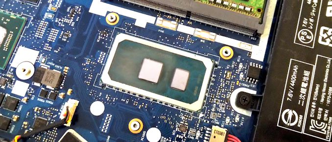
Anyone interested in leading edge semiconductors knows that Intel is late with its newest manufacturing process. The '10nm' node was first announced in 2014, to be released in 2016. While officially 'shipping for revenue' by 31 December 2017, the only way we knew to get hold of an Intel 10nm x86 CPU was if you happened to be a Chinese school and work with a specific distributor to buy a specific laptop.We pulled in a few favors from within the industry and managed to source the laptop for review.
Intel's Sole 10nm Processor
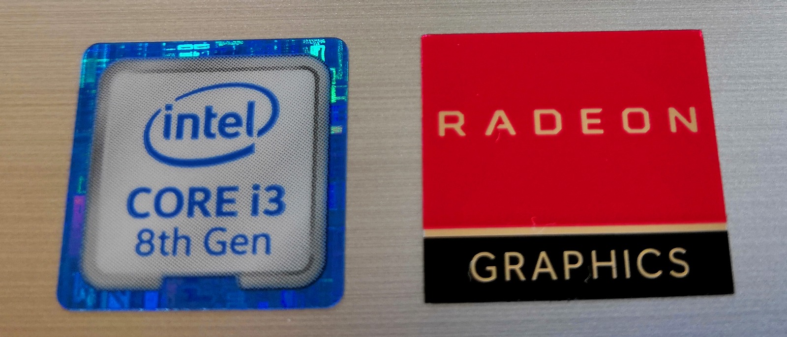
The single processor from Intel built on 10nm falls under the Core 8th generation family, and is called the Core i3-8121U. The cores are built with Intel's Cannon Lake microarchitecture, a variant of the Skylake architecture built on 14nm, and it is manufactured as a dual core with integrated graphics. The part nominally has a standard 'GT2' graphics configuration, but is actually shipped without the graphics enabled - some analysts believe that this is because it doesn't work (see more on the next page). Norminally this is a 2+2 design (two cores, GT2 graphics), however it might also be referred to as a 2+0 design.
| Intel 10nm Cannon Lake CPUs | ||||||
| Cores | Base Freq |
Turbo Freq |
Graphics | DRAM | TDP | |
| Core i3-8121U | 2 (4) | 2.2 GHz | 3.2 GHz | None (GT2 Fused Off) |
DDR4-2400 LPDDR4-2400 |
15W |
The two cores run at a 2.2 GHz base frequency at 15W thermal design power, and offers a 3.2 GHz turbo frequency. Memory support includes LPDDR4, one of very few Intel processors to do so, but also this processor has AVX-512 capabilities, allowing it to process vector math much like Intel's Enterprise class hardware but now in a low end chip. We'll dive deep into all these points in this review.
What Do We Have
The sole laptop which has an Intel Core i3-8121U inside is a specific model of the Chinese Lenovo Ideapad E330-15ICN.

The advert from the listing
This is an educational focused device, with educational focused specifications - a 15.6-inch screen running at a 1366x768 resolution with a TN panel (with limited viewing angles), a small 33.4 Wh battery, 8GB of DRAM, a 256GB SSD, and a 1TB mechanical hard-drive. Because the chip has no integrated graphics, Lenovo had to add a physical GPU, which will be the same one as found in the upcoming NUC: AMD's Radeon RX540. This adds another 50W thermal design power to the whole unit, which complicates the cooling system considerably compared to a standard 15W CPU on its own. Along the educational theme, it also comes with an ethernet port, a HDMI port, two USB ports, a 3.5mm jack, a Type-C USB connector, a 720p webcam, a microSD card slot, an 802.11ac Wi-Fi module, and an optional DVD slot (which loses the second SATA HDD).
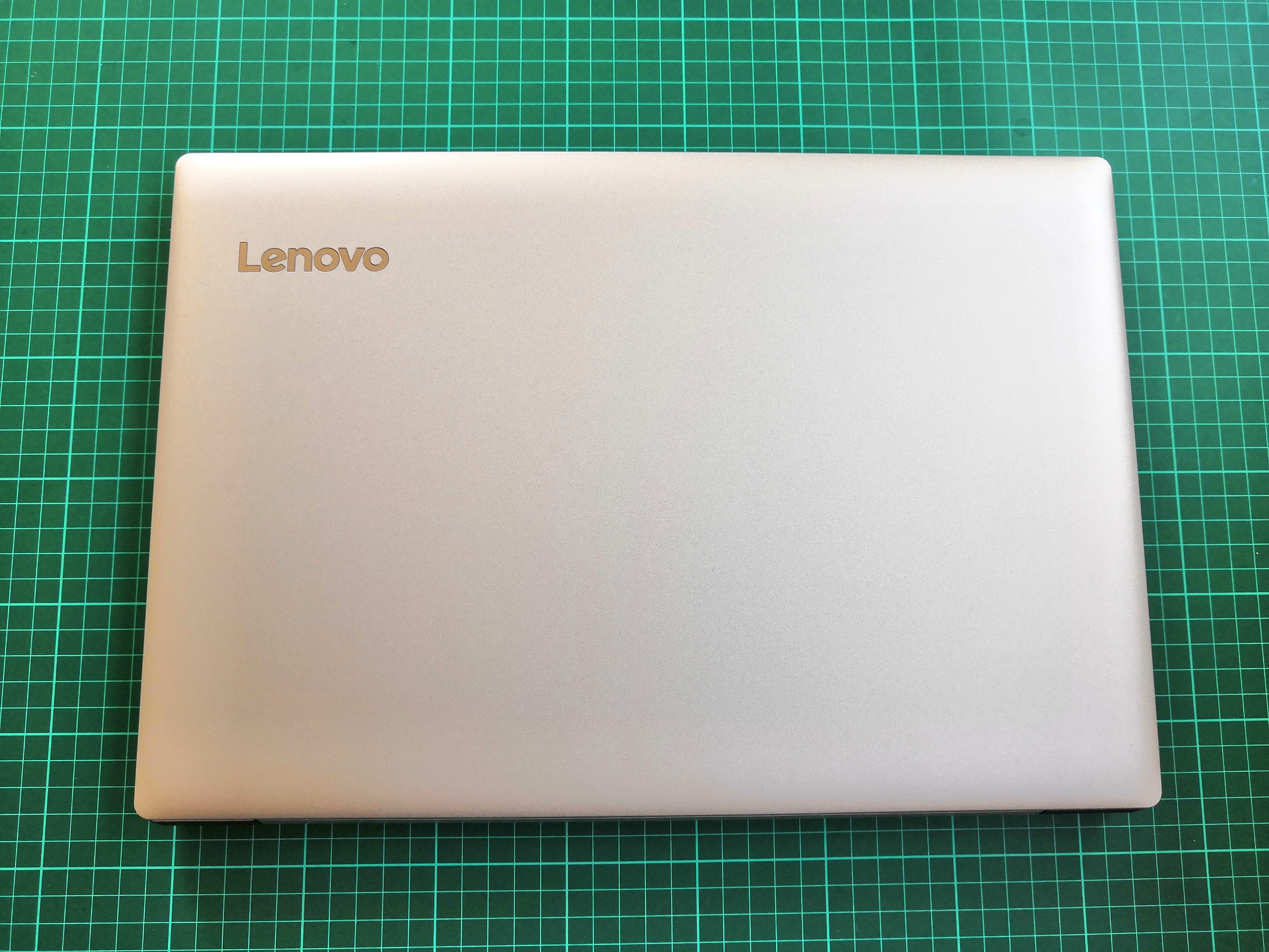
The design is very unassuming. The grey finish means that it won't stand out at Starbucks, aside from the bulk of a heavy 15.6-inch device. As is perhaps to be expected, it feels very utilitarian. No-one is buying this for looks or for style.
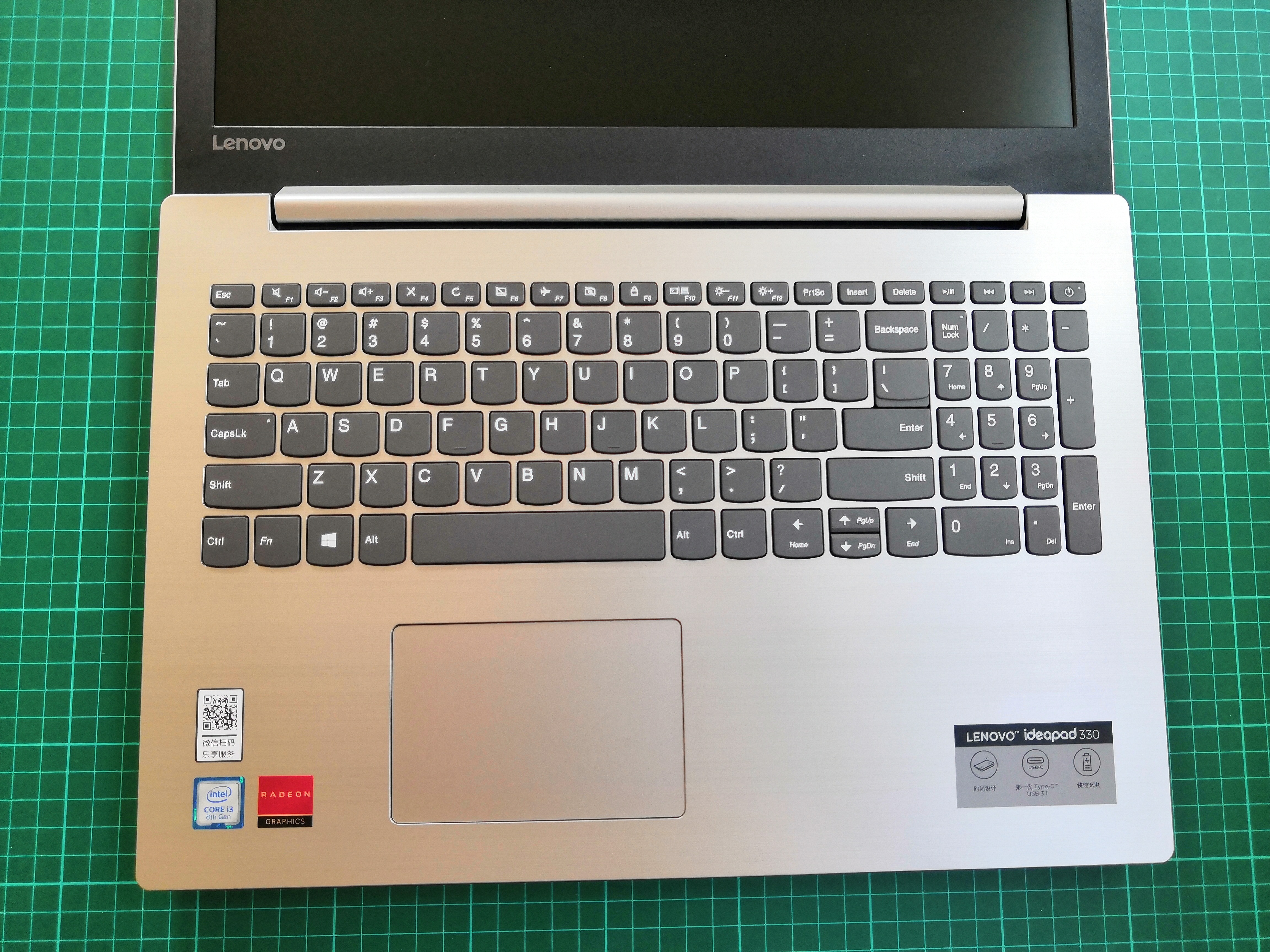
The keyboard fits in with the cost-down implementation here, although having used it for a few events to take notes, it is very usable. Despite being a Chinese device, we ended up with a US keyboard, but with half-height arrow buttons. The keypad is also present, with some media keys at the top. Unfortunately the power key is on the top right, above the minus sign, making it very easy to hit for prolific users of a keypad.

On the top is the webcam. This unit has massive bezels for the display, which contributes a lot to the bulk of the system. The webcam is usable for meetings at least, and the microphones do work but are cheap as we expect.

Welcome to the heart - Intel Core i3 plus AMD Radeon graphics. Sadly not an impressive combination like Kaby G.
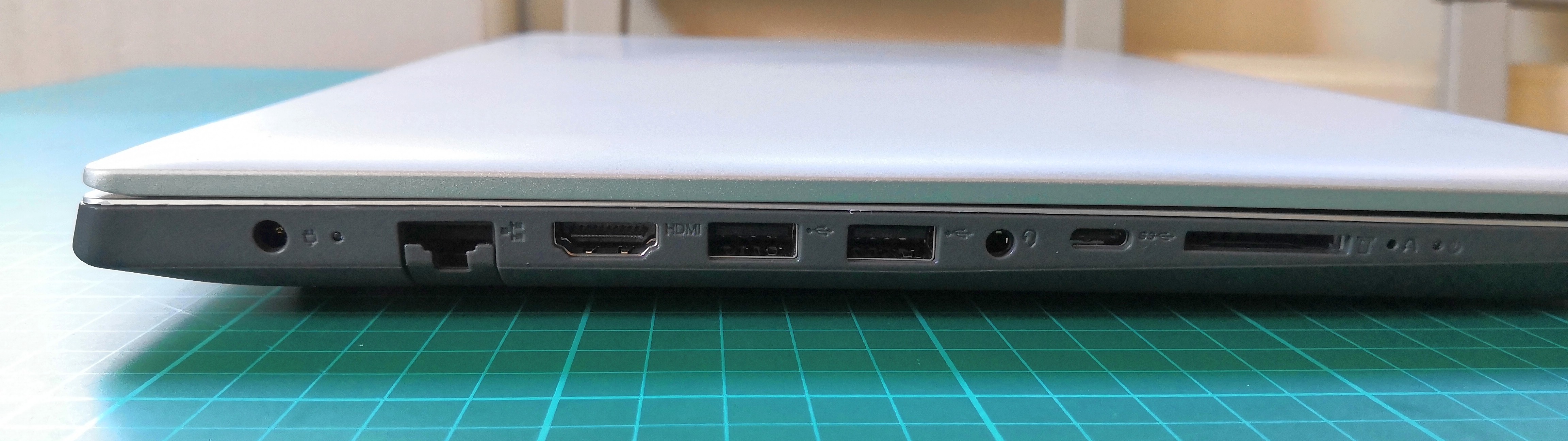
On the sides are all of the ports. They are all located on the left side, and include the power connector, the gigabit Ethernet port, a HDMI port, two USB ports, a 3.5mm jack, a Type-C USB port, and an SD card slot. On the other side of the unit is the removable bay.
On the rear, we get intakes at the front, and an intake in the middle of the bottom of the chassis. There are small rubber feet to help lift the laptop when on a table, but these do not really help on a lap. Given the amount of heat that needs to be dissipated in this system, this isn't great - the exhaust is found in the hinge between the main body and the display. The fan inside has to cope with all of this, as we'll see in a bit.

Going inside the system, and removing the removable bay, looks a bit like this.
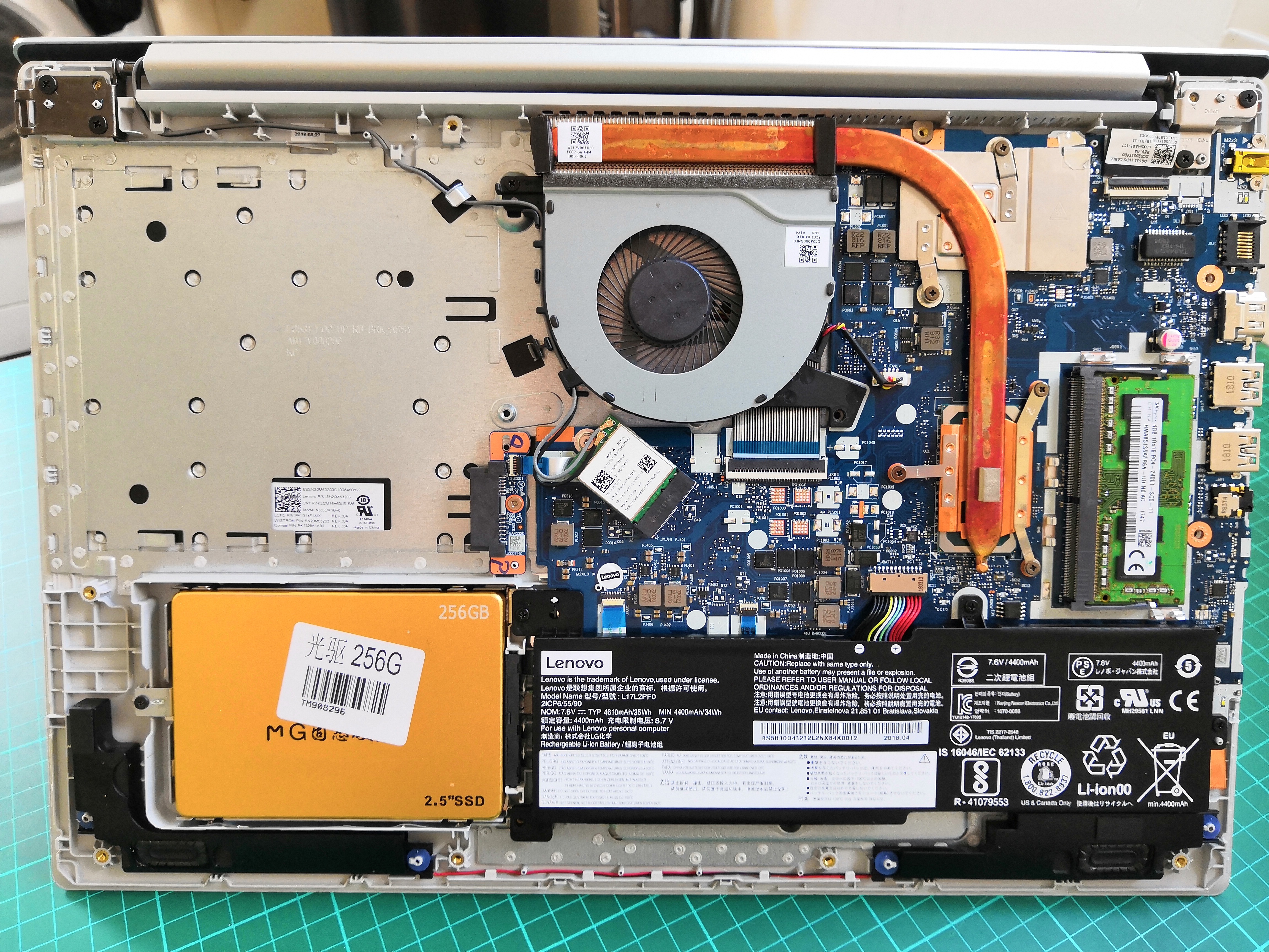
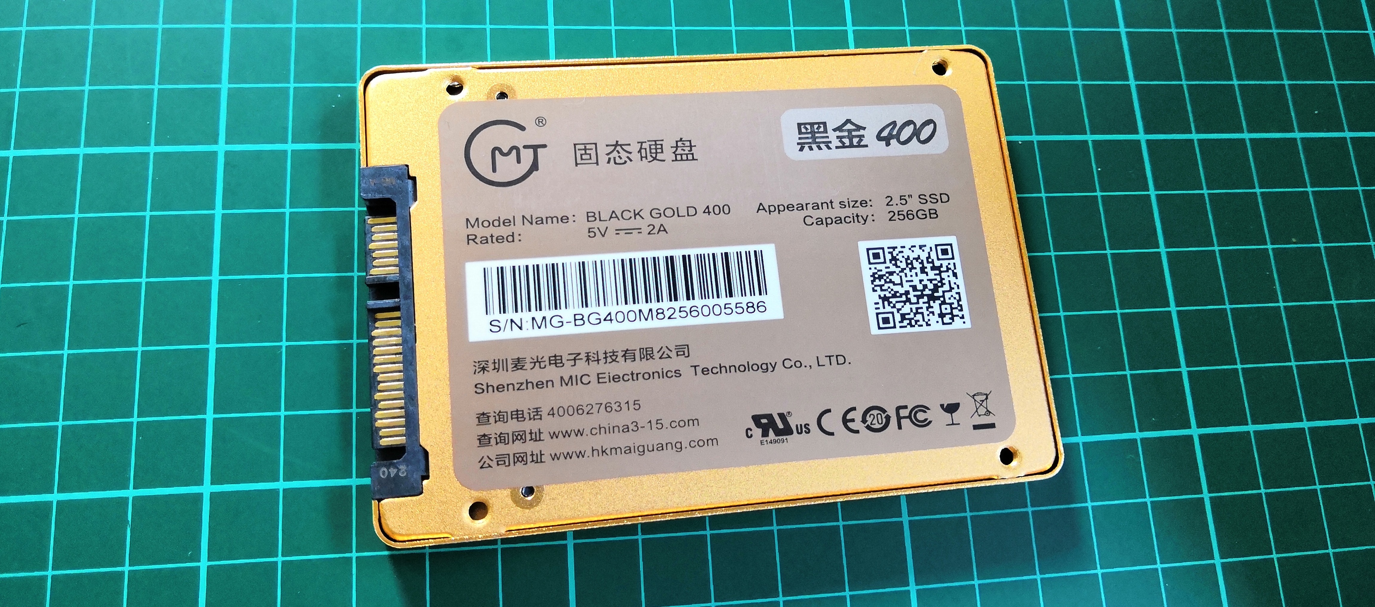
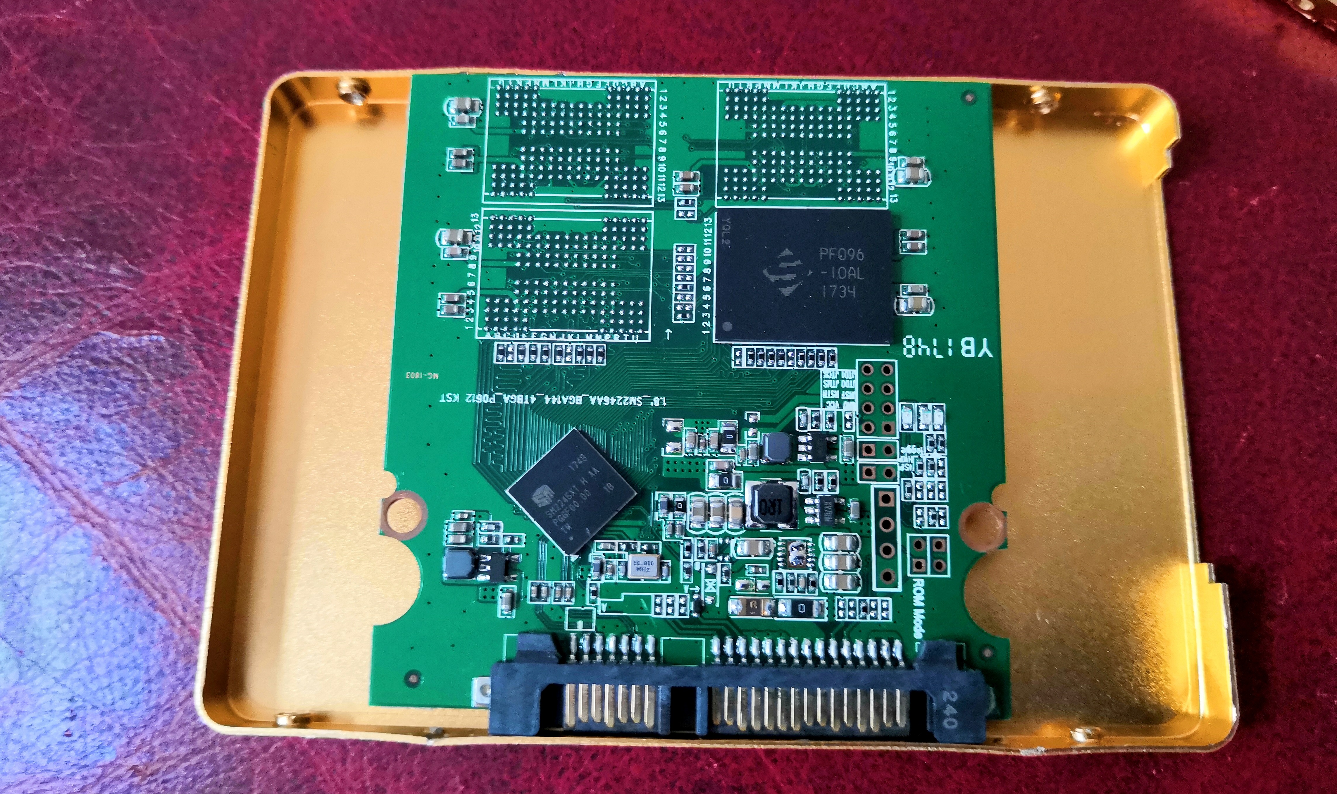
On the left is the 256GB SSD, branded as an 'MT Black Gold 400' drive in a 2.5-inch chassis. This unit is very gold. It is a budget drive, featuring the DRAM-less Silicon Motion SM2246XT controller combined with Spektek NAND flash (rebadged cheap Micron NAND). This unit is clearly part of a series of SSDs, given the number of empty pads. But I guess even having an SSD is still an interesting upgrade over a purely mechanical drive.
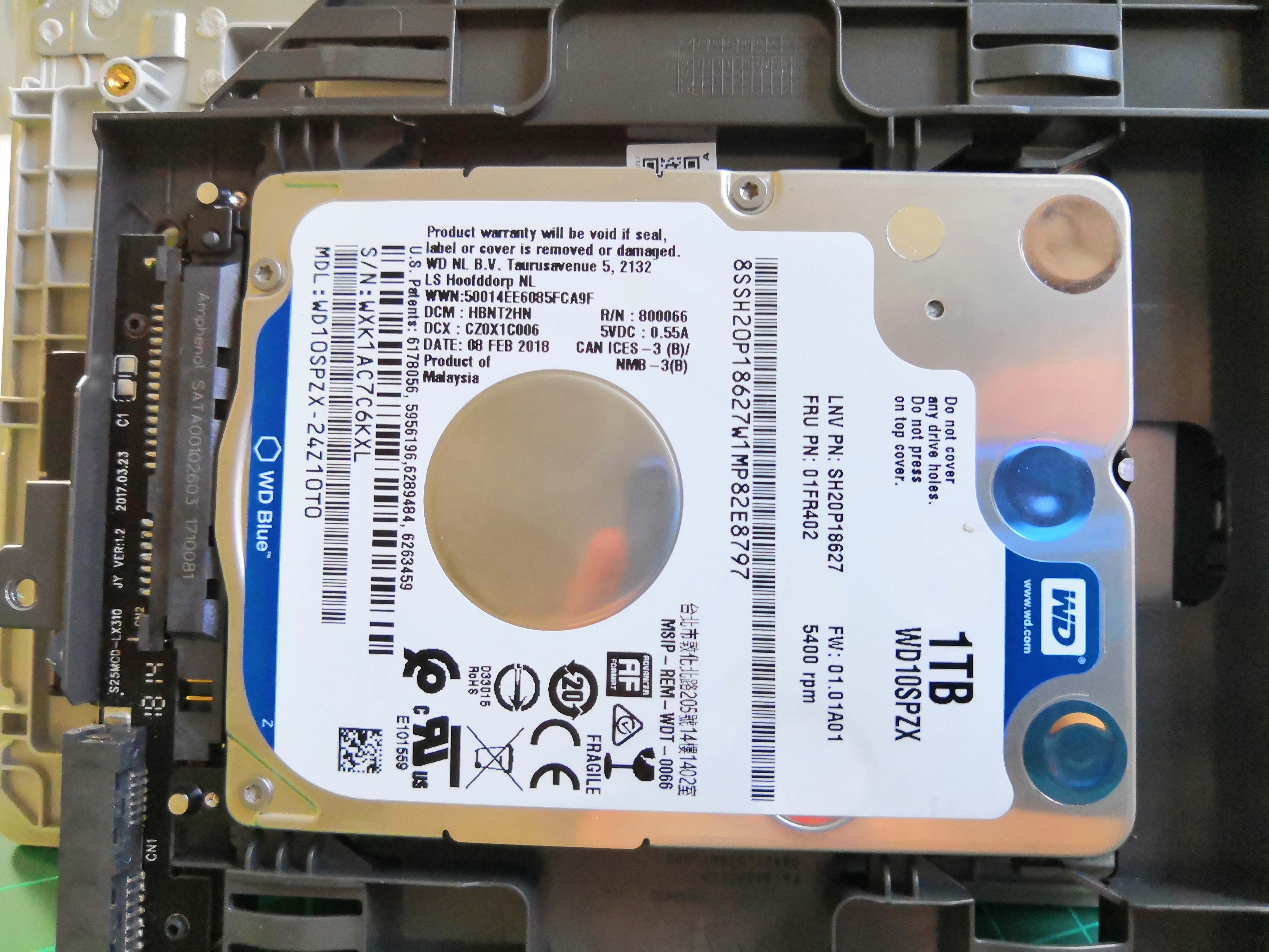
The other drive in the system, not pictured in the main image, is spinning rust - a 1TB WD Blue. This is actually pretty commendable to have this drive in a system like this, although the 5400RPM platter speed means that it will be slow for almost everything. It makes me wonder if drives like this should be using the SSD as a caching technology instead.
The WiFi module has a Lenovo part number but underneath is a Realtek RTL8821CE 802.11ac module, supporting 433 Mbps speed (1T1R) and Bluetooth. This is an M.2 module, which means it could be upgraded at a later date fairly easily. It is a dual band module, which as an educational system should be more than suitable for the classroom that has an access point close by.

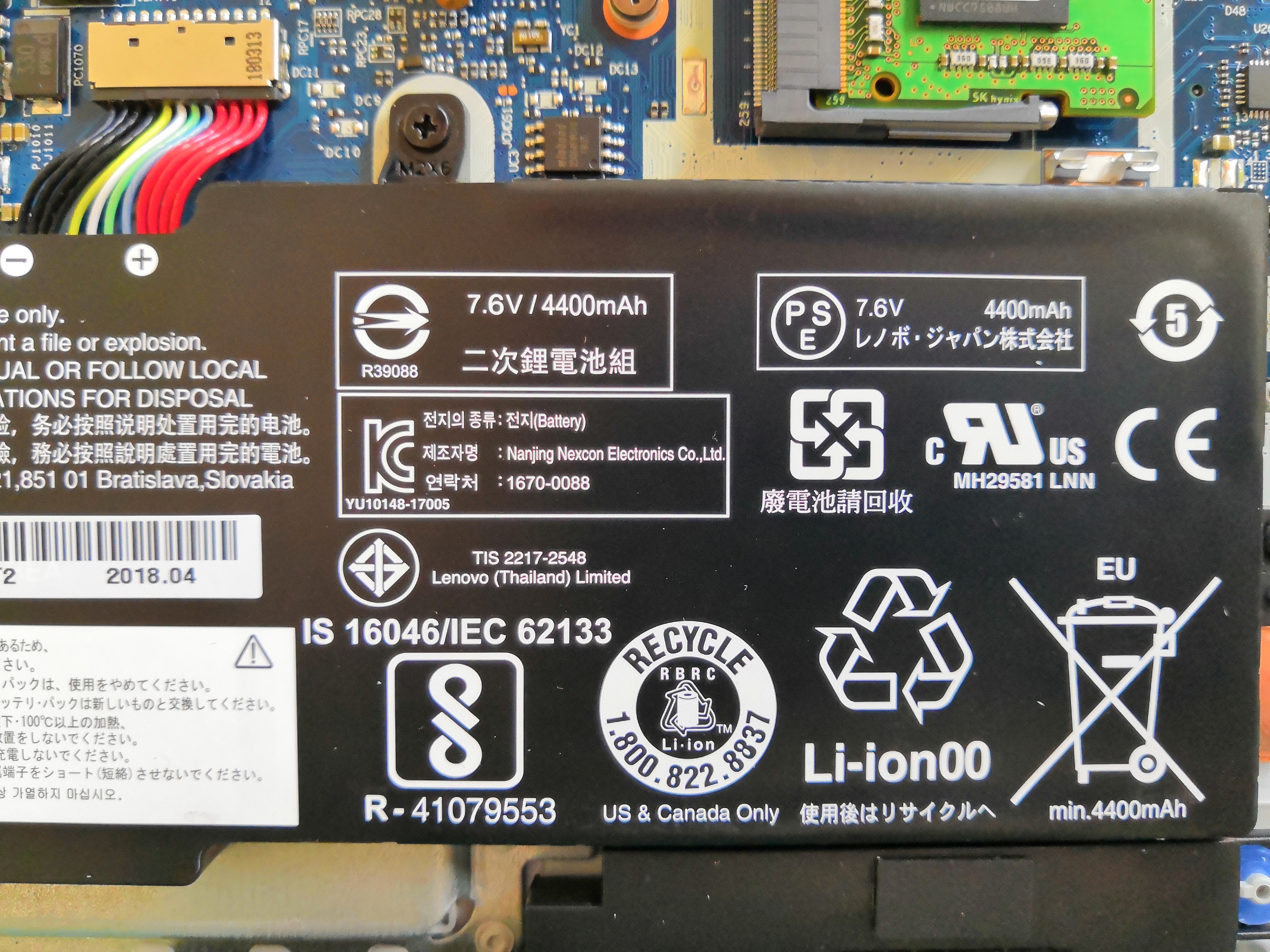
The battery, as mentioned above, is a tiny battery. The 33.4Wh lithium-ion unit is a 2-cell device, which equates to 4400 mAh at 7.6 V, and is made for Lenovo in Thailand by the Nanjing Nexcon Electronics Co.
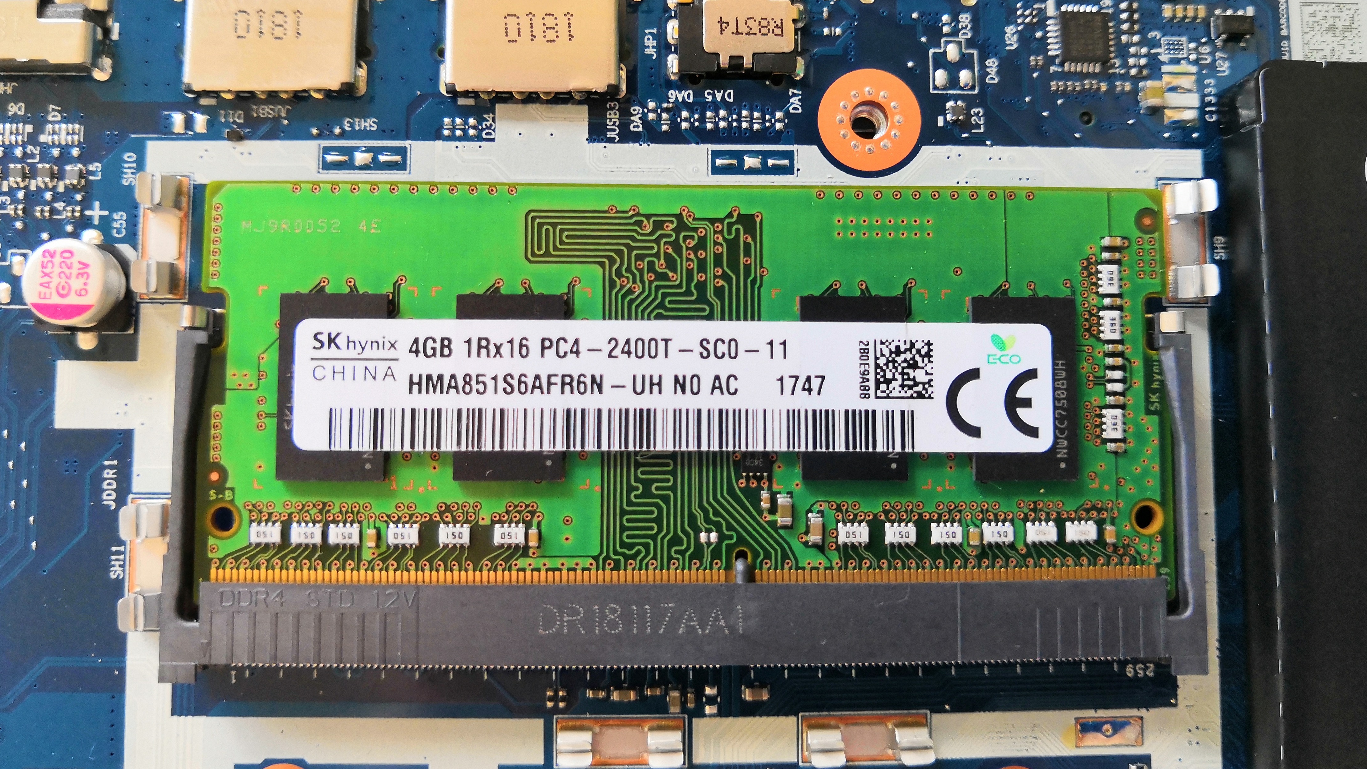
For system memory, the unit has 4GB soldered onto the rear of the PCB, and offers a single SO-DIMM slot for an additional module. The base configuration for this device has 4GB of memory in single channel mode, however up to 16GB more can be added. The configurations we were offered showed another 4GB module, bringing the total up to 8GB. Again, having 8GB of DRAM in an educational device probably sits about right, and kudos for them being in dual channel as well.
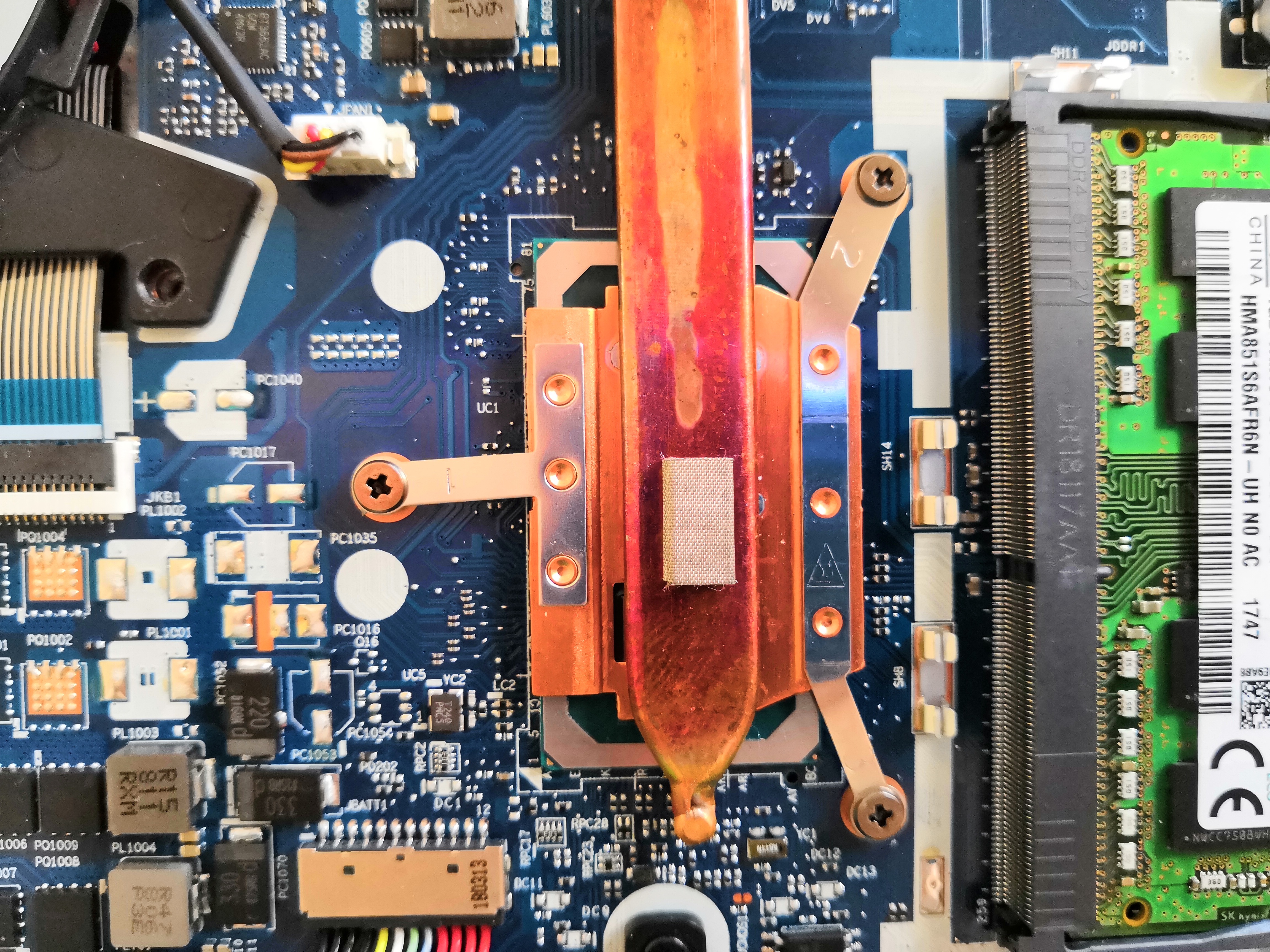
The meat of the laptop, the CPU and GPU, are found near the center and have blower cooling. Despite the 15W TDP of the CPU and the 50W TDP of the GPU, there is a single flat heatpipe going from the CPU to the GPU and to the heatsink connected to the thin blower fan. This feels like a cheap fan paired with aluminum fins. This feels woefully inadequate for such the system, and the power consumption combined with the small battery leads to interesting figures for battery life. In thermals, the system does get warm to the touch around the cooler area, which is thankfully a little way away from the keyboard and not really felt when active.
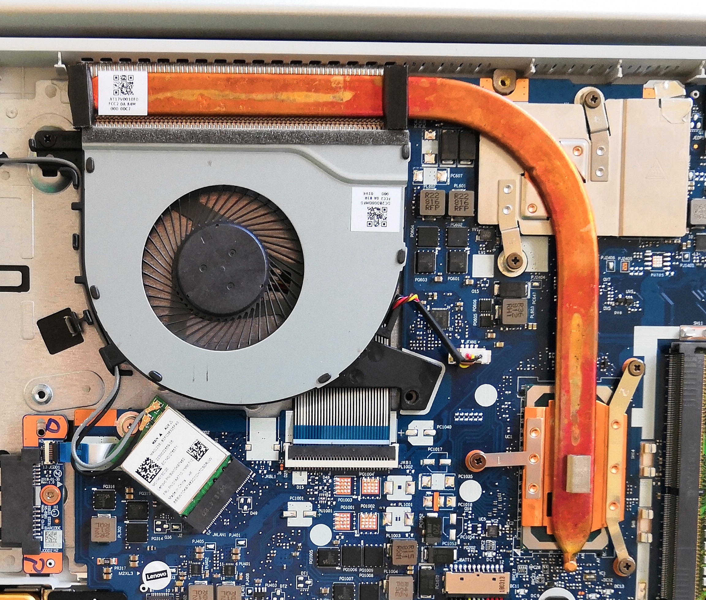
The GPU area has a sizable copper heatsink fixed in two spots to the PCB.
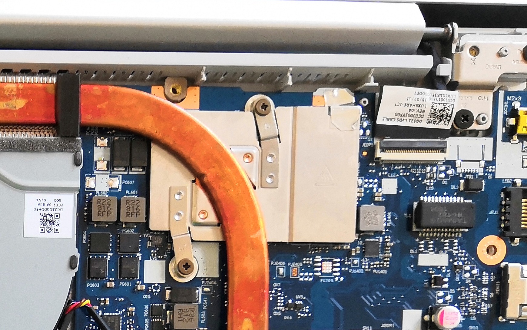
The CPU area is instead attached at three points, and there is an additional pad to stop the chassis from rubbing against the heatpipe. This means that the chip height combined with the PCB and the heatsink is enough to start to worry how the chassis brushes up against the internals? Interesting.
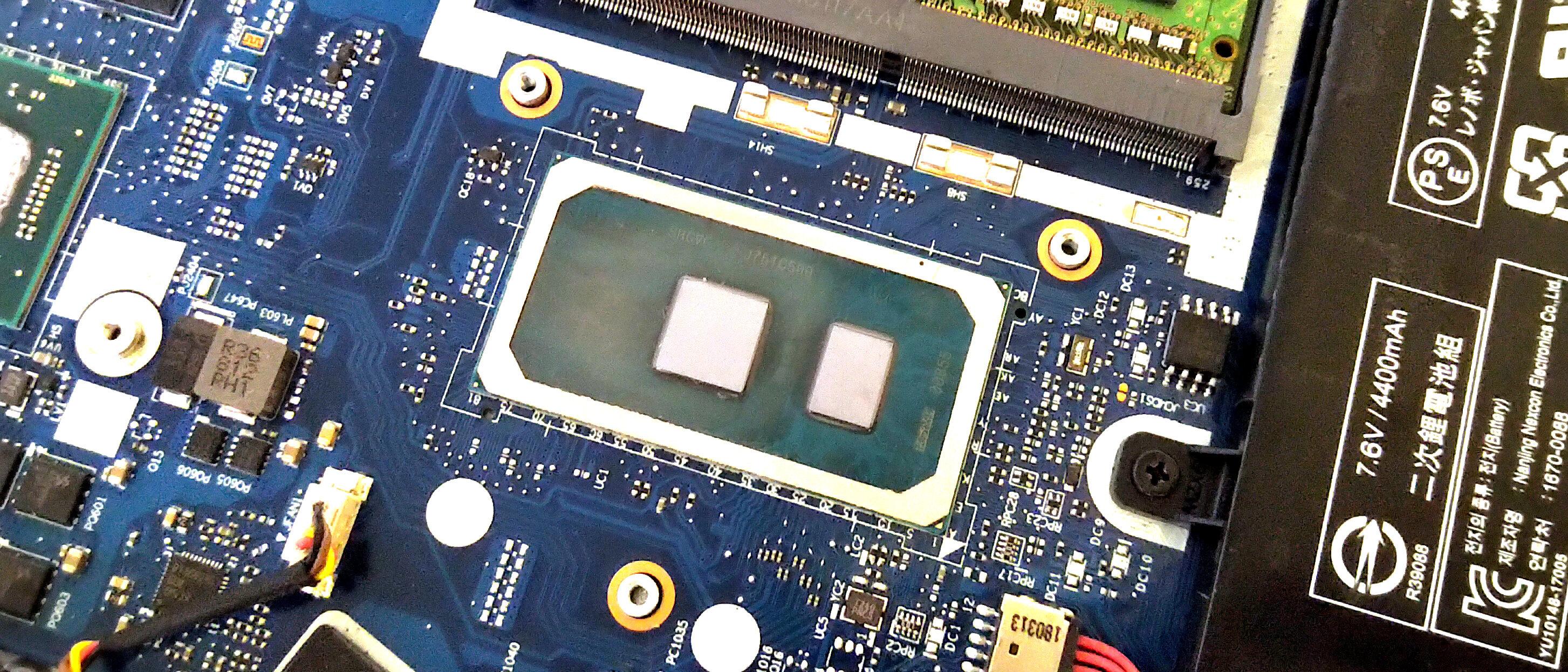
Underneath the heatsink is this chip. What we have here is the 2+2 die from Intel (with graphics disabled, so 2+0 as shipped), along with the chipset. Back when Intel showed off a full wafer of these chips, we calculated a rough die size of 8.2mm by 8.6mm, or 70.5mm2 per die. In actual fact, we were essentially accurate in our estimation. This means there can be up to 850 dies per 300mm wafer. How many of those actually work at the level Intel wanted? That would be a fun question to have answered.
The base model of this device retailed for around $450 from our source in China - that's the 4GB model with a 500GB HDD. With the extra memory (up to 8GB) and storage (256GB SSD + 1TB HDD) the cost to us was around $650, plus postage. It took about six weeks to get the device, after calling in a few favors from friends in the region. For everyone else, a NUC was recently released onto shelves in December.
This Review
Within this article we want to do several things. Firstly, discuss and describe the history behind Intel's 10nm plans, the claims and the marketing, as well as what we currently know about what is in this 10nm Cannon Lake processor. Then we will go into what Cannon Lake brings to the table in its microarchitecture based on what we can find out, using tools, microbenchmarks, and also calling in some investigative experts. Following this is some benchmarks - we want to look into both generational improvements and chip production performance increases, coming at the performance angle but also a nod towards power and memory performance. Finally we'll end with a discussion about the future of this version of Intel's 10nm.
It should be noted that Intel did not offer or provide the device for this article - we purchased this device ourselves. When asked about diving deeper into the design of the chip about a month ago, Intel never really responded to my request. I currently have a more recent request to discuss the topic, and I'm waiting on a response.


129 Comments
View All Comments
eva02langley - Sunday, January 27, 2019 - link
Even better...https://youtu.be/osSMJRyxG0k?t=1220
AntonErtl - Sunday, January 27, 2019 - link
Great Article! The title is a bit misleading given that it is much more than just a review. I found the historical perspective of the Intel processes most interesting: Other reporting often just reports on whatever comes out of the PR department of some company, and leaves the readers to compare for themselves with other reports; better reporting highlights some of the contradictions; but rarely do we se such a pervasive overview.The 8121U would be interesting to me to allow playing with AVX512, but the NUC is too expensive for me for that purpose, and I can wait until AMD or Intel provide it in a package with better value for money.
RamIt - Sunday, January 27, 2019 - link
Need gaming benches. This would make a great cs:s laptop for my daughter to game with me on.Byte - Monday, January 28, 2019 - link
Cannonlake, 2019's Broadwell.f4tali - Monday, January 28, 2019 - link
I can't believe I read this whole review from start to finish...And all the comments...
And let it sink in for over 24hrs...
But somehow my main takeaway is that 10nm is Intel's biggest graphics snafu yet.
(Well THAT and the fact you guys only have one Steam account!)
;)
NikosD - Monday, January 28, 2019 - link
@Ian CutressGreat article, it's going to become all-time classic and kudos for mentioning semiaccurate and Charlie for his work and inside information (and guts)
But really, how many days, weeks or even months did it take to finish it ?
bfonnes - Monday, January 28, 2019 - link
RIP IntelCharonPDX - Monday, January 28, 2019 - link
Insane to think that there have been as many 14nm "generations" as there were "Core architecture" generations before 14nm.ngazi - Tuesday, January 29, 2019 - link
Windows is snappy because there is no graphics switching. Any machine with the integrated graphics completely off is snappier.Catalina588 - Wednesday, January 30, 2019 - link
@Ian, This was a valuable article and it is clipped to Evernote. Thanks!Without becoming Seeking Alpha, you could add another dimension or two to the history and future of 10nm: cost per transistor and amortizing R&D costs. At Intel's November 2013 investor meeting, William Holt strongly argued that Intel would deliver the lowest cost per transistor (slide 13). Then-CFO Stacey Smith and other execs also touted this line for many quarters. But as your article points out, poor yields and added processing steps make 10nm a more expensive product than the 14nm++ we see today. How will that get sold and can Intel improve the margins over the life of 10nm?
Then there's amortizing the R&D costs. Intel has two independent design teams in Oregon and Israel. Each team in the good-old tick-tock days used to own a two-year process node and new microarchitecture. The costs for two teams over five-plus years without 10nm mainstream products yet is huge--likely hundreds of millions of dollars. My understanding is that Intel, under general accounting rules, has to write off the R&D expense over the useful life of the 10nm node, basically on a per chip basis. Did Intel start amortizing 10nm R&D with the "revenue" for Cannon Lake starting in 2017, or is all of the accrued R&D yet to hit the income statement? Wish I knew.
Anyway, it sure looks to me like we'll be looking back at 10nm in the mid-2020s as a ten-year lifecycle. A big comedown from a two-year TickTock cycle.