Sizing Up Servers: Intel's Skylake-SP Xeon versus AMD's EPYC 7000 - The Server CPU Battle of the Decade?
by Johan De Gelas & Ian Cutress on July 11, 2017 12:15 PM EST- Posted in
- CPUs
- AMD
- Intel
- Xeon
- Enterprise
- Skylake
- Zen
- Naples
- Skylake-SP
- EPYC
Intel Expanding the Chipset: 10 Gigabit Ethernet and QuickAssist Technology
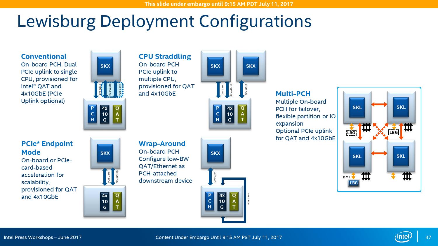
The refresh strategy from Intel on the chipset side has an ultra-long cadence. In recent memory, Intel’s platform launches are designed to support two generations of processor release, and in that time there is typically no chipset update, leaving the platform controller hub semi-static for functionality for usually three years. This is compared to the consumer side, where new chipsets are launched with every new CPU generation, with bigger jumps coming every couple of years. For the new launch today, Intel pushing the enterprise chipset ahead in a new direction.
The point of the chipset previously was to provide some basic IO support in the form of SATA/SAS ports, some USB ports, and a few PCIe lanes for simple controllers like USB 3.0, Gigabit Ethernet, or perhaps an x4 PCIe slot for a non-accelerator type card. The new chipsets, part of the C620 family codenamed Lewisburg, are designed to assist with networking, cryptography, and act more like a PCIe switch with up to 20 PCIe 3.0 lane support.
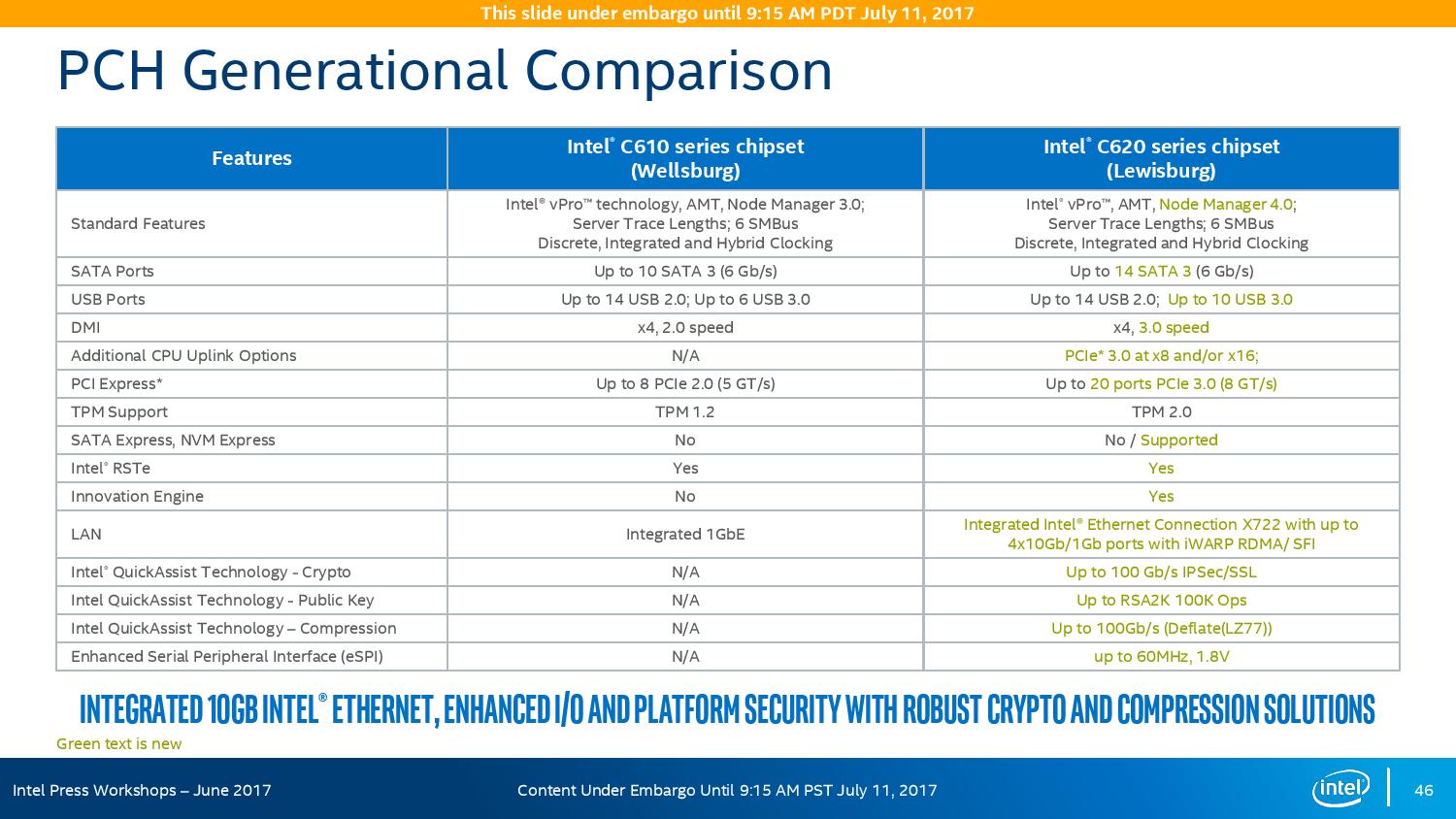
The headline features that matter most is the upgrade in DMI connection to the chipset, upgraded from DMI 2.0 to DMI 3.0 to match the consumer platforms, having those 20 PCIe 3.0 lanes from the chipset, and also the new feature under CPU Uplink.
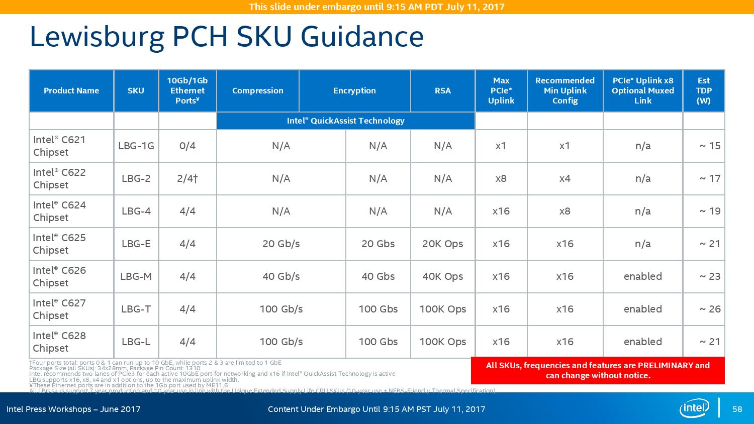
For the new generation of Lewisburg chipsets, if an OEM requires that a platform has access to a cryptography engine or 10 Gigabit Ethernet, then they can attach 8 or 16 lanes from the processor into the chipset via this CPU Uplink port. Depending on which model of chipset is being used, this can provide up to four 10 GbE ports with iWARP RDMA, or up to 100 GB/s IPSec/SSL of QuickAssist support.
Intel will offer seven different versions of the chipset, varying in 10G and QAT support, but also varying in TDP:
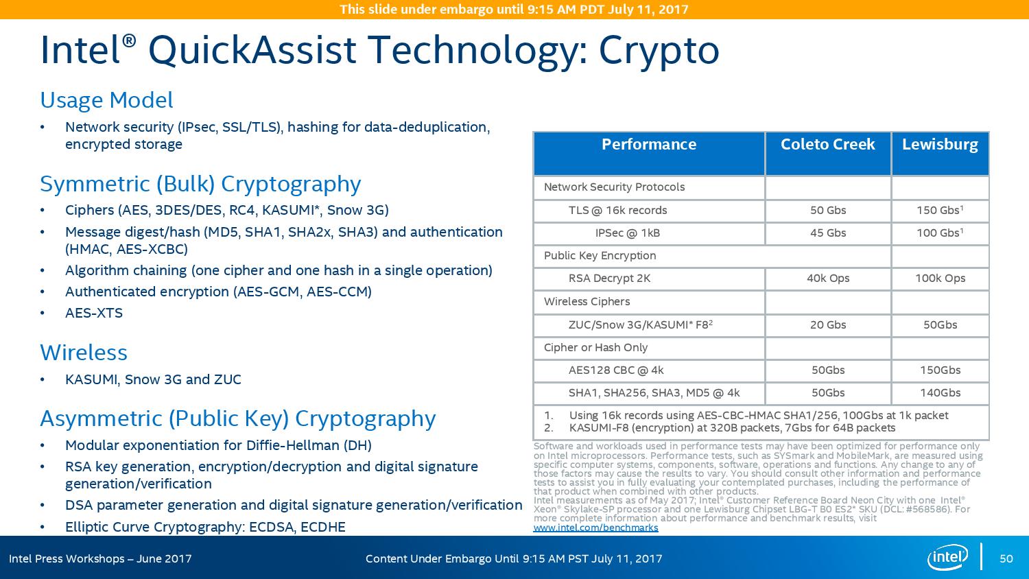
On the cryptography side, Intel has previously sold add-in PCIe cards for QuickAssist, but is now moving it onto the systems directly. By adding it into the chipset, it can be paired with the Ethernet traffic and done in-situ, and specifically Intel points to bulk cryptography (150 Gb/s AES256/SHA256), Public Key Encryption (100k ops of RSA2048) and compression (100+ Gb/s deflate).
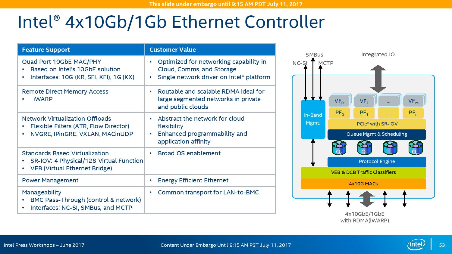
With the GbE, Intel has designed this to be paired with the X722 PHY, and supports network virtualization, traffic shaping, and supports Intel’s Data Plane Development Kit for advanced packet forwarding.
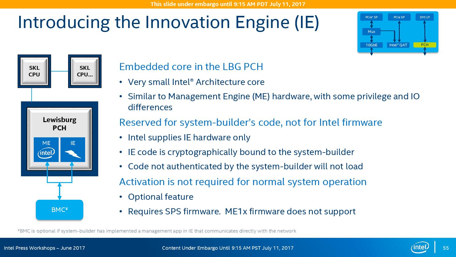
The chipset will also include a new feature called Intel’s Innovation Engine, giving a small embedded core into the PCH which mirrors Intel’s Management Engine but is designed for system-builders and integrators. This allows specialist firmware to manage some of the capabilities of the system on top of Intel’s ME, and is essentially an Intel Quark x86 core with 1.4MB SRAM.
The chipsets are also designed to be supported between different CPUs within the same multi-processor system, or for a system to support multiple chipsets at once as needed.


219 Comments
View All Comments
TheOriginalTyan - Tuesday, July 11, 2017 - link
Another nicely written article. This is going to be a very interesting next couple of months.coder543 - Tuesday, July 11, 2017 - link
I'm curious about the database benchmarks. It sounds like the database is tiny enough to fit into L3? That seems like a... poor benchmark. Real world databases are gigabytes _at best_, and AMD's higher DRAM bandwidth would likely play to their favor in that scenario. It would be interesting to see different sizes of transactional databases tested, as well as some NoSQL databases.psychobriggsy - Tuesday, July 11, 2017 - link
I wrote stuff about the active part of a larger database, but someone's put a terrible spam blocker on the comments system.Regardless, if you're buying 64C systems to run a DB on, you likely will have a dataset larger than L3, likely using a lot of the actual RAM in the system.
roybotnik - Wednesday, July 12, 2017 - link
Yea... we use about 120GB of RAM on the production DB that runs our primary user-facing app. The benchmark here is useless.haplo602 - Thursday, July 13, 2017 - link
I do hope they elaborate on the DB benchmarks a bit more or do a separate article on it. Since this is a CPU article, I can see the point of using a small DB to fit into the cache, however that is useless as an actual DB test. It's more an int/IO test.I'd love to see a larger DB tested that can fit into the DRAM but is larger than available caches (32GB maybe ?).
ddriver - Tuesday, July 11, 2017 - link
We don't care about real world workloads here. We care about making intel look good. Well... at this point it is pretty much damage control. So let's lie to people that intel is at least better in one thing.Let me guess, the databse size was carefully chosen to NOT fit in a ryzen module's cache, but small enough to fit in intel's monolithic die cache?
Brought to you by the self proclaimed "Most Trusted in Tech Since 1997" LOL
Ian Cutress - Tuesday, July 11, 2017 - link
I'm getting tweets saying this is a severely pro AMD piece. You are saying it's anti-AMD. ¯\_(ツ)_/¯ddriver - Tuesday, July 11, 2017 - link
Well, it is hard to please intel fanboys regardless of how much bias you give intel, considering the numbers.I did not see you deny my guess on the database size, so presumably it is correct then?
ddriver - Tuesday, July 11, 2017 - link
In the multicore 464.h264ref test we have 2670 vs 2680 for the xeon and epyc respectively. Considering that the epyc score is mathematically higher, howdoes it yield a negative zero?Granted, the difference is a mere 0.3% advantage for epyc, but it is still a positive number.
Headley - Friday, July 14, 2017 - link
I thought the exact same thing