AMD Zen Microarchiture Part 2: Extracting Instruction-Level Parallelism
by Ian Cutress on August 23, 2016 8:45 PM EST- Posted in
- CPUs
- AMD
- x86
- Zen
- Microarchitecture
Hot Chips is an annual conference that allows semiconductor companies to present their latest and greatest ideas or forthcoming products in an academic-style environment, and is predominantly aimed as the professional semiconductor engineer. This year has a number of talks about power management, upcoming IBM CPUs, upcoming Intel CPUs, upcoming NVIDIA SoCs and the final talk of the final day is from AMD, discussing Zen in even more depth than the previous week. While we were unable to attend the event in person, we managed to get some hands on time with information and put questions to Mike Clark, AMD Senior Fellow and design engineer.
What We Learned Last Week: L1/L2/L3 Caches and the Micro-Op Buffer
In AMD’s initial presentation for the general media, we were given a sense of the microarchitecture layout. We covered the material, but it contained a number of highlights.
AMD Zen Microarchitecture: Dual Schedulers, Micro-op Cache and Memory Hierarchy Revealed
AMD Server CPUs and Motherboard Analysis
Unpacking AMD's Zen Benchmark: Is Zen actually 2% Faster than Broadwell?
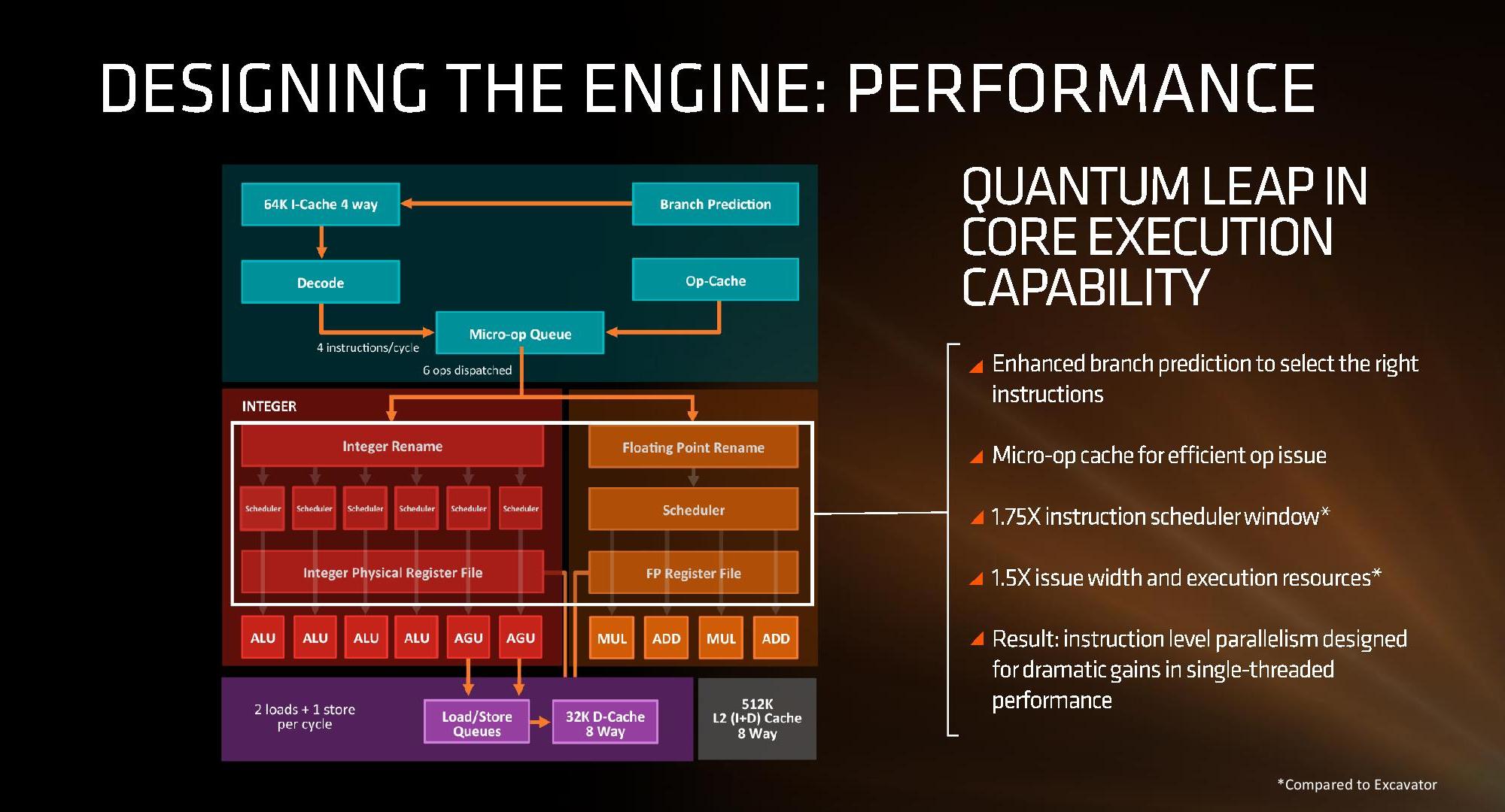
First up, and the most important, was the announcement of the inclusion of a micro-op cache. This allows for instructions that are frequently used to be closer to the micro-op queue and saves a trip through the core and caches to load the desired information. Typically micro-op caches are still relatively small, and while AMD isn’t giving any information for size and accessibility, we know that Intel’s version can support 1536 uOps with 8-way associativity; we expect AMD’s to be similar though there are many options in play.
Secondly is the cache structure. We were given details for the L1, L2 and L3 cache sizes, along with associativity, to compare it to former microarchitectures as well as Intel’s offering.
| CPU Cache Comparison | |||||
| Zen HEDT |
Bulldozer HEDT |
Excavator |
Skylake | Broadwell HEDT |
|
| L1-I | 64KB/core | 64KB/module | 96KB/module | 32KB/core | 32KB/core |
| 4-way | 2-way | 3-way | 8-way | 8-way | |
| L1-D | 32KB/core | 16KB/thread | 32KB/thread | 32KB/core | 32KB/core |
| 8-way | 4-way | 8-way | 8-way | 8-way | |
| L2 | 512KB/core | 1MB/thread | 512KB/thread | 256KB/core | 256KB/core |
| 8-way | 16-way | 16-way | 4-way | 8-way | |
| L3 | 2MB/core | 1MB/thread | - | >2MB/core | 1.5-3MB/core |
| 16-way | 64-way | - | 16-way | 16/20-way | |
| L3 Type | Victim | Victim | - | Write-back | Write-back |
In this case, AMD has given Zen a 64KB L1 Instruction cache per core with 4-way associativity, with a lop-sided 32KB L1 Data cache per core with 8-way associativity. The size and accessibility determines how frequently a cache line is missed, and it is typically a trade-off for die area and power (larger caches require more die area, more associativity usually costs power). The instruction cache, per cycle, can afford a 32byte fetch while the data cache allows for 2x 16-byte loads and one 16-byte store per cycle. AMD stated that allowing two D-cache loads per cycle is more representative of the most workloads that end up with more loads than stores.
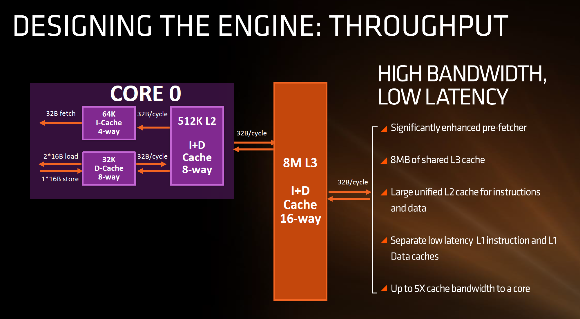
The L2 is a large 512 KB, 8-way cache per core. This is double the size of Intel’s 256 KB 4-way cache in Skylake or 256 KB 8-way cache in Broadwell. Typically doubling the cache size affords a 1.414 (square root of 2) better chance of a cache hit, reducing the need to go further out to find data, but comes at the expense of die area. This will have a big impact on a lot of performance metrics, and AMD is promoting faster cache-to-cache transfers than previous generations. Both the L1 and L2 caches are write-back caches, improving over the L1 write-through cache in Bulldozer.
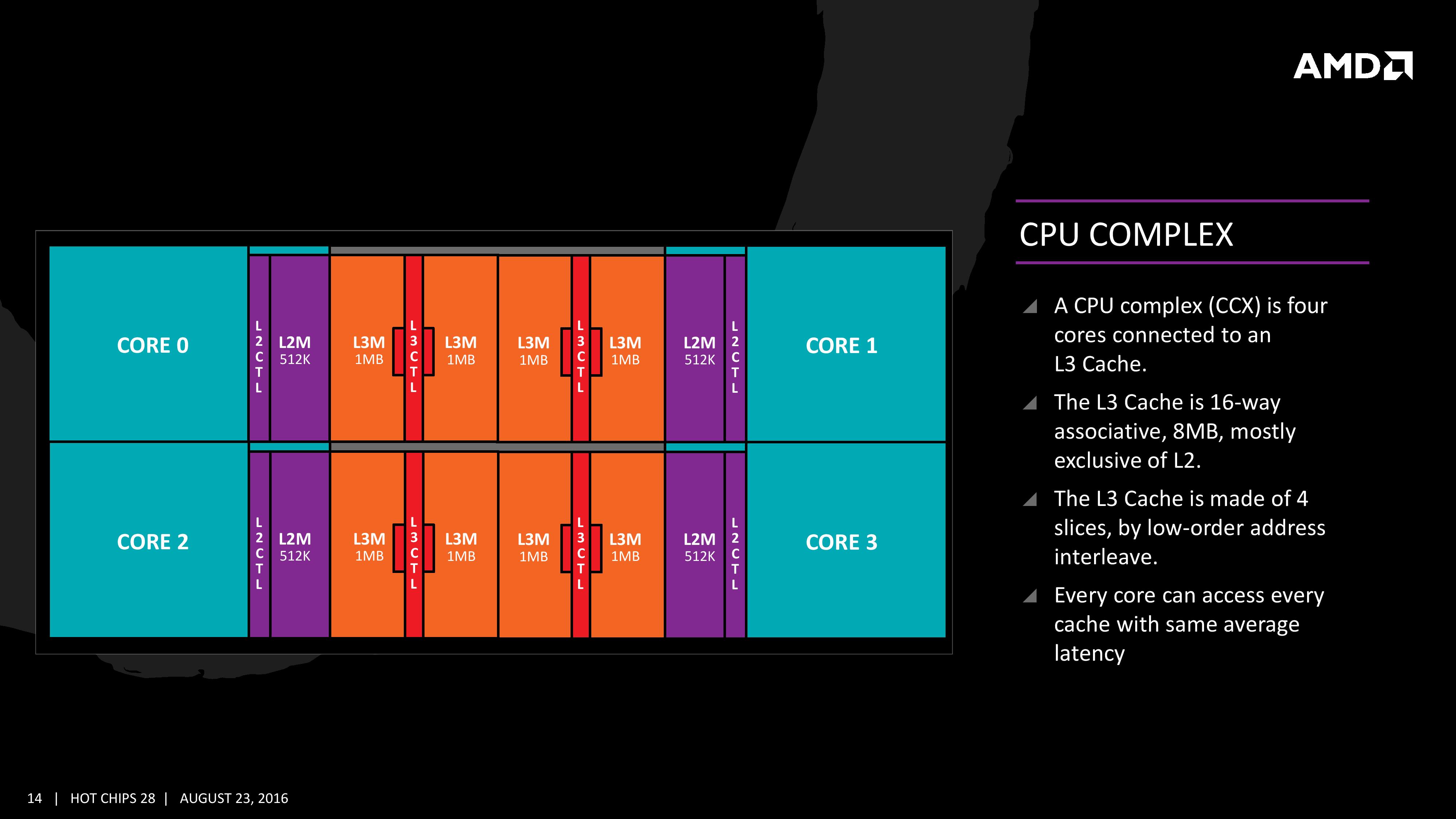
The L3 cache is an 8MB 16-way cache, although at the time last week it was not specified over how many cores this was. From the data release today, we can confirm rumors that this 8 MB cache is split over a four-core module, affording 2 MB of L3 cache per core or 16 MB of L3 cache for the whole 8-core Zen CPU. These two 8 MB caches are separate, so act as a last-level cache per 4-core module with the appropriate hooks into the other L3 to determine if data is needed. As part of the talk today we also learned that the L3 is a pure victim cache for L1/L2 victims, rather than a cache for prefetch/demand data, which tempers the expectations a little but the large L2 will make up for this. We’ll discuss it as part of today’s announcement.
The mid-week release also gave insight into the dual schedulers, one for INT and another for FP, which is different to Intel’s joint scheduler/buffer implementation. The talk at Hot Chips goes into detail about how the dispatch and schedulers operate
The New Information
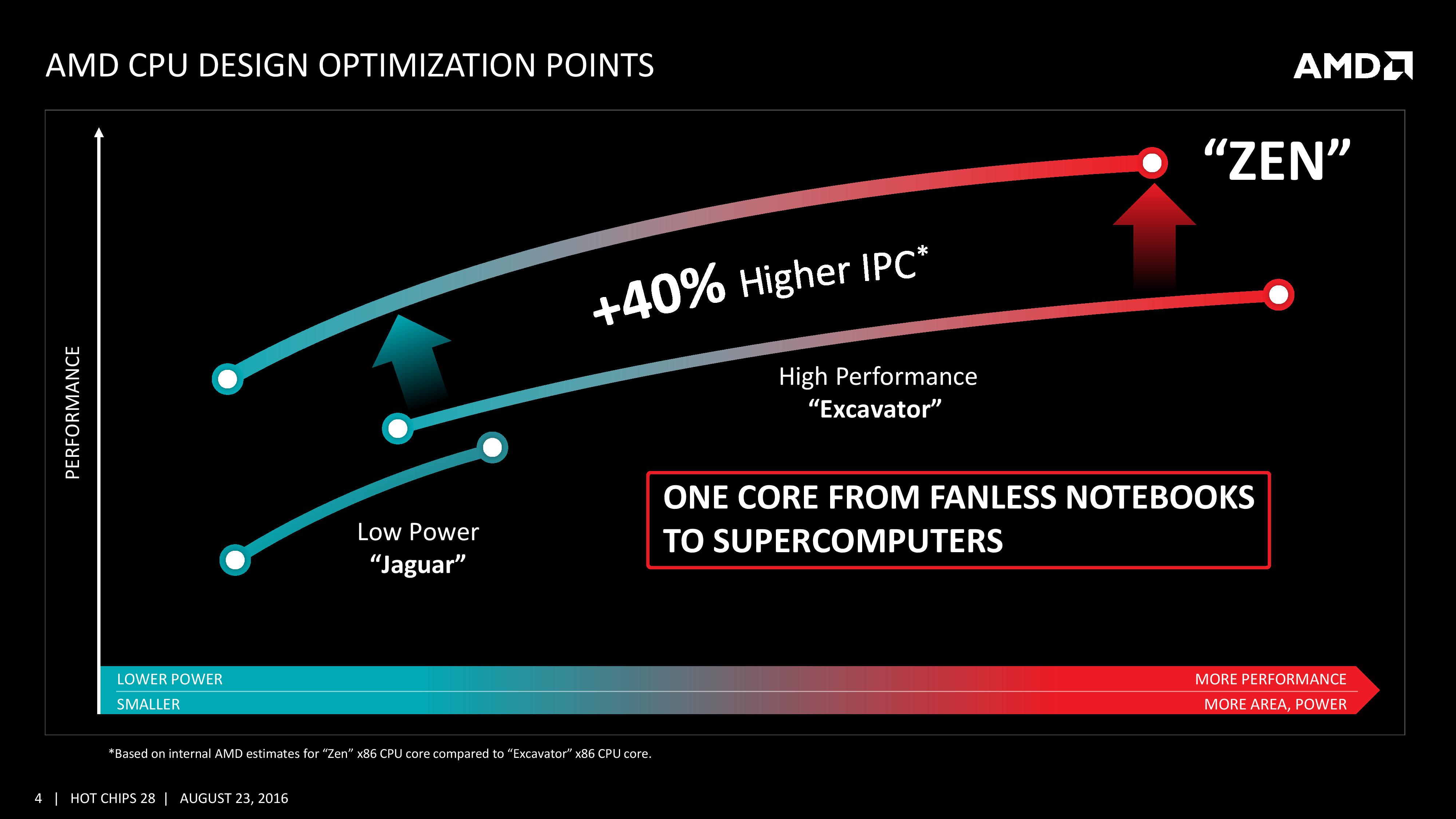
As part of the Hot Chips presentation, AMD is reaffirming its commitment to at least +40% IPC improvement over Excavator. This has specifically been listed as a throughput goal at an equivalent energy per cycle, resulting in an increase in efficiency. Obviously a number of benefits come from moving the 28nm TSMC process to GloFo’s 14nm FinFET process which is used via a Samsung licence. Both the smaller node and FinFET improvements have been well documented so we won’t go over them here, but AMD is stating that Zen is much more than this as a direct improvement to immediate performance, not just efficiency. While Zen is initially a high-performance x86 core at heart, it is designed to scale all the way from notebooks to supercomputers, or from where the Cat cores (such as Jaguar and Puma) were all the way up to the old Opterons and beyond, all with at least +40% IPC.
The first immediate image out of the presentation is the CPU Complex (a CCX), which shows the Zen core design as a four-CPU cluster with caches. This shows the L2/L3 cache breakdown, and also confirms 2MB of L3 per core with 8 MB of L3 per CCX. It also states that the L3 is mostly exclusive of the L2 cache, which stems from the L3 cache as a victim cache for L2 data. AMD is stating that the protocols involved in the L3 cache design allow each core to access the L3 of each other core with an average (but a range) of latencies.
Over the next few pages, we’ll go through the slides. They detail more information about the application of Simultaneous Multithreading (SMT), New Instructions, the size of various queues and buffers, the back-end of the design, the front-end of the design, fetch, decode, execute, load/store and retire segments.


106 Comments
View All Comments
eldakka - Wednesday, August 24, 2016 - link
The first page link, AMD Server CPUs and Motherboard Analysis, is wrong, it actually links to the ARM v8-A article.atlantico - Friday, August 26, 2016 - link
Yes, it's also wrong here: http://www.anandtech.com/show/10585/unpacking-amds...Sigh.
TristanSDX - Wednesday, August 24, 2016 - link
Zen do not support transactional memory, big disadvantage comparing to IntelSenti - Wednesday, August 24, 2016 - link
And how much does it matter? TSX is great thing no doubt there. But the adoption? What can you name of real software what uses and get significant benefit of it?I blame Intel stupid marketing for cutting TSX from too many versions and killing the adoption.
coder111 - Wednesday, August 24, 2016 - link
As far as I know, Azul JVMs do support transactional memory. So if you have a Java app, you can use it.Other than that, yes, I haven't seen TSX used much...
68k - Wednesday, August 24, 2016 - link
Isn't the version of glibc in recent Linux-distributions using the lock elision feature of TSX?https://lwn.net/Articles/534758/
https://01.org/blogs/tlcounts/2014/lock-elision-gl...
If so, then essentially every single Linux program does make use of TSX when present.
looncraz - Wednesday, August 24, 2016 - link
One of the most important features of TSX are checkpoints. Zen supports checkpoints in its execution pipeline. Otherwise, I've not seen anything that said Zen did or did not support TSX, not that the tech is widely used at this time.From there, you just need tagging and a few other features to add support. It's something that could be included in Zen+ if Zen does not have it.
silverblue - Wednesday, August 24, 2016 - link
It looks like Zen was developed to accelerate the vast majority of software, and rely on core count for everything else. It might explain the lack of focus on AVX.If cache stats were any indication of performance, it would appear that Zen was destined to compete with Broadwell, but not quite match the Lake CPUs; Zen+ would perhaps close the gap albeit a bit late. Bulldozer was hamstrung by half-speed writes and horrific L3 latency - would it be remiss to assume that they've at least fixed those two issues?
I'm not sure anybody can truly predict performance however, even with a Blender demonstration, and certainly not to work out prospective Cinebench or SuperPi performance. You could have a monster of an architecture, but if the software isn't optimised for it, it's not going to be representative of its true performance.
wumpus - Wednesday, August 24, 2016 - link
I'd still want the TSX instructions before even thinking about the server market. I guess they surrendered that before the overall architecture was finished. Although considering how badly it has worked for Intel (essentially turned off after errata was noted in the first generation), maybe it wasn't worth risk.Alexvrb - Sunday, August 28, 2016 - link
Yeah they need to take their time. A faulty implementation would do more harm than good at this point.