The NVIDIA GeForce GTX 1080 & GTX 1070 Founders Editions Review: Kicking Off the FinFET Generation
by Ryan Smith on July 20, 2016 8:45 AM ESTFeeding Pascal: GDDR5X
An ongoing problem for every generation of GPUs is the matter of memory bandwidth. As graphics is an embarrassingly parallel problem, it scales out with additional ALUs – and consequently Moore’s Law – relatively well. Each successive generation of GPUs are wider and higher clocked, consuming more data than ever before.
The problem for GPUs is that while their performance tracks Moore’s Law well, the same cannot be said for DRAM. To be sure, DRAM has gotten faster over the years as well, but it hasn’t improved at nearly the same pace as GPUs, and physical limitations ensure that this will continue to be the case. So with every generation, GPU vendors need to be craftier and craftier about how they get more memory bandwidth, and in turn how they use that memory bandwidth.
To help address this problem, Pascal brings to the table two new memory-centric features. The first of which is support for the newer GDDR5X memory standard, which looks to address the memory bandwidth problem from the supply side.
By this point GDDR5 has been with us for a surprisingly long period of time – AMD first implemented it on the Radeon HD 4870 in 2008 – and it has been taken to higher clockspeeds than originally intended. Today’s GeForce GTX 1070 and Radeon RX 480 cards ship with 8Gbps GDDR5, a faster transfer rate than the originally envisioned limit of 7Gbps. That GPU manufacturers and DRAM makers have been able to push GDDR5 so high is a testament to their abilities, but at the same time the technology is clearly reaching its apex (at least for reasonable levels of power consumption)
As a result there has been a great deal of interest in the memory technologies that would succeed GDDR5. At the high end, last year AMD became the first vendor to implement version 1 of High Bandwidth Memory, a technology that is a significant departure from traditional DRAM and uses an ultra-wide 4096-bit memory bus to provide enormous amounts of bandwidth. Not to be outdone, NVIDIA has adopted HBM2 for their HPC-centric GP100 GPU, using it to deliver 720GB/sec of bandwidth for Pascal P100.
While from a technical level HBM is truly fantastic next-generation technology – it uses cutting edge technology throughput, from TSV die-stacking to silicon interposers that connect the DRAM stacks to the processor – its downside is that all of this next-generation technology is still expensive to implement. Precise figures aren’t publicly available, but the silicon interposer is more expensive than a relatively simple PCB, and connecting DRAM dies through TSVs and stacking them is more complex than laying down BGA DRAM packages on a PCB. For NVIDIA, a more cost-effective solution was desired for GP104.
That solution came from Micron and the JEDEC in the form of GDDR5X. A sort of half-generation extension of traditional GDDR5, GDDR5X further increases the amount of memory bandwidth available from GDDR5 through a combination of a faster memory bus coupled with wider memory operations to read and write more data from DRAM per clock. And though it’s not without its own costs such as designing new memory controllers and boards that can accommodate the tighter requirements of the GDDR5X memory bus, GDDR5X offers a step in performance between the relatively cheap and slow GDDR5, and relatively fast and expensive HBM2.
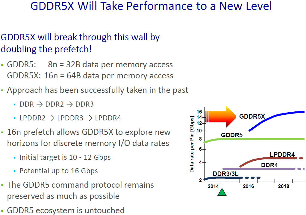
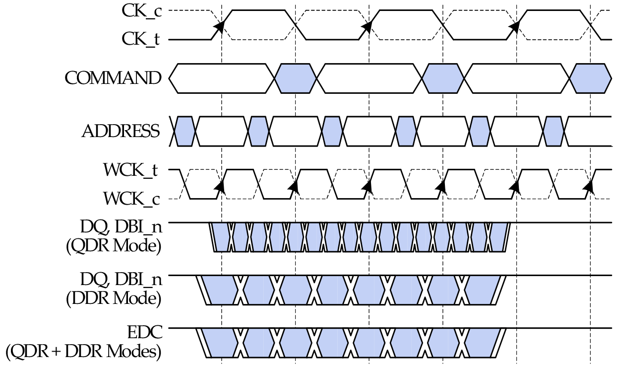
Relative to GDDR5, the significant breakthrough on GDDR5X is the implementation of Quad Data Rate (QDR) signaling on the memory bus. Whereas GDDR5’s memory bus would transfer data twice per write clock (WCK) via DDR, GDDR5X extends this to four transfers per clock. All other things held equal, this allows GDDR5X to transfer twice as much data per clock as GDDR5.
QDR itself is not a new innovation – Intel implemented a quad pumped bus 15 years ago for the Pentium 4 with AGTL+ – but this is the first time it has been implemented in a common JEDEC memory standard. The history of PC memory standards is itself quite a tale, and I suspect that the fact we’re only seeing a form of QDR now is related to patents. But regardless, here we are.
Going hand-in-hand with the improved transfer rate of the GDDR5X memory bus, GDDR5X also once again increases the size of read/write operations, as the core clockspeed of GDDR5X chips is only a fraction of the bus speed. GDDR5X uses a 16n prefetch, which is twice the size of GDDR5’s 8n prefetch. This translates to 64B reads/writes, meaning that GDDR5X memory chips are actually fetching (or writing) data in blocks of 64 bytes, and then transmitting it over multiple cycles of the memory bus. As discussed earlier, this change in the prefetch size is why the memory controller organization of GP104 is 8x32b instead of 4x64b like GM204, as each memory controller can now read and write 64B segments of data via a single memory channel.
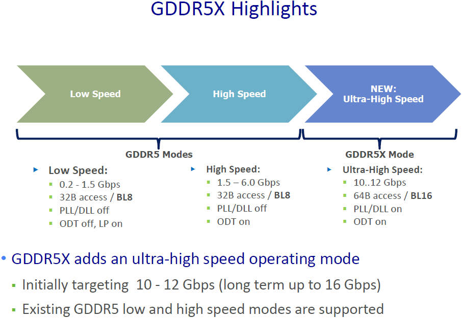
Overall GDDR5X is planned to offer enough bandwidth for at least the next couple of years. The current sole supplier of GDDR5X, Micron, is initially developing GDDR5X from 10 to 12Gbps, and the JEDEC has been talking about taking that to 14Gbps. Longer term, Micron thinks the technology can hit 16Gbps, which would be a true doubling of GDDR5’s current top speed of 8Gbps. With that said, even with a larger 384-bit memory bus (ala GM200) this would only slightly surpass what kind of bandwidth HBM2 offers today, reinforcing the fact that GDDR5X will fill the gap between traditional GDDR5 and HBM2.
Meanwhile when it comes to power consumption and power efficiency, GDDR5X will turn back the clock, at least a bit. Thanks in large part to a lower operating voltage of 1.35v, circuit design changes, and a smaller manufacturing node for the DRAM itself, 10Gbps GDDR5X only requires as much power as 7Gbps GDDR5. This means that relative to GTX 980, GTX 1080’s faster GDDR5X is essentially “free” from a power perspective, not consuming any more power than before, according to NVIDIA.
That said, while this gets NVIDIA more bandwidth for the same power – 43% more, in fact – NVIDIA has now put themselves back to where they were with GTX 980. GDDR5X can scale higher in frequency, but doing so will almost certainly further increase power consumption. As a result they are still going to have to carefully work around growing memory power consumption if they continue down the GDDR5X path for future, faster cards.
On a final specification note, GDDR5X also introduces non-power-of-two memory chip capacities such as 12Gb. These aren’t being used for GTX 1080 – which uses 8Gb chips – but I wouldn’t be surprised if we see these used down the line. The atypical sizing would allow NVIDIA to offer additional memory capacities without resorting to asymmetrical memory configurations as is currently the case, all the while avoiding the bandwidth limitations that can result from that.
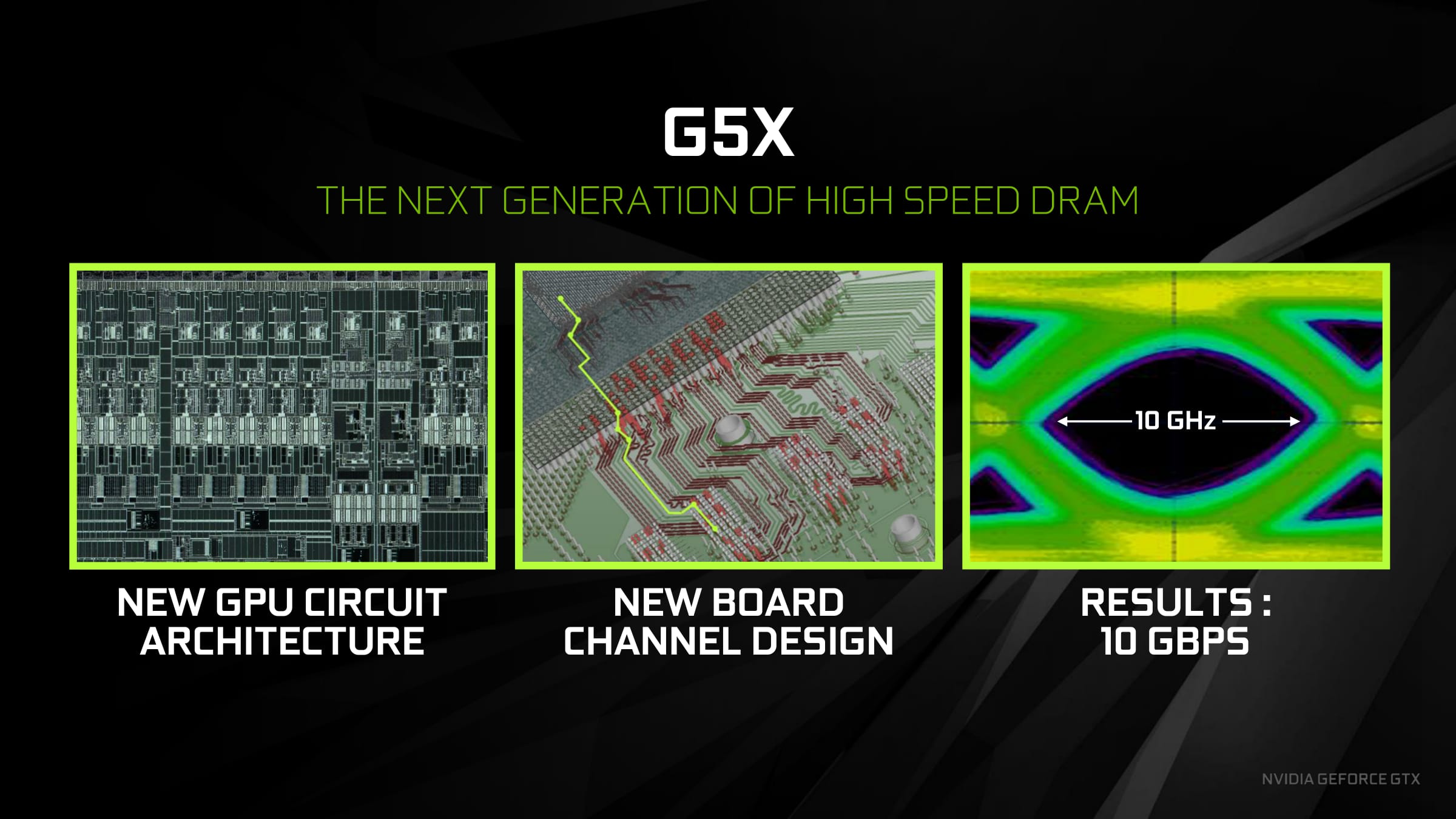
Moving on to implementation details, GP104 brings with it a new memory controller design to support GDDR5X. As intended with the specification, this controller design is backwards compatible with traditional GDDR5, and will allow NVIDIA to support both memory standards. At this point NVIDIA hasn’t talked about what kinds of memory speeds their new controller can ultimately hit, but the cropped signal analysis diagram published in their slide deck shows a very tight eye. Given the fact that NVIDIA’s new memory controller can operate at 8Gbps in GDDR5 mode, I would be surprised if we don’t see at least 12Gbps GDDR5X by the tail-end of Pascal’s lifecycle.
But perhaps the bigger challenge is on the board side of matters, where NVIDIA and their partners needed to develop PCBs capable of handling the tighter signaling requirements of the GDDR5X memory bus. At this point video cards are moving 10Gbps/pin over a non-differential bus, which is itself a significant accomplishment. And keep in mind that in the long run, the JEDEC and Micron want to push this higher still.
To that end it somewhat undersells the whole process to just say that GDDR5X required “tighter signaling requirements”, but it’s an apt description. There is no single technology in place on the physical trace side to make this happen; it’s just a lot of precision, intensive work into ensuring that the traces and the junctions between the PCB, the chip, and the die all retain the required signal integrity. With a 256-bit wide bus we’re not looking at something too wide compared to the 384 and 512-bit buses uses on larger GPUs, so the task is somewhat simpler in that respect, but it’s still quite a bit of effort to minimize the crosstalk and other phenomena that degrade the signal, and which GDDR5X has little tolerance for.
As it stands I suspect we have not yet seen the full ramifications of the tighter bus requirements, and we probably won’t for cards that use the reference board or the memory design lifted from the reference board. For stability reasons, data buses are usually overengineered, and it’s likely the GDDR5X memory itself that’s holding back overclocking. Things will likely get more interesting if and when GDDR5X filters its way down to cheaper cards, where keeping costs in check and eking out higher margins becomes more important. Alternatively, as NVIDIA’s partners get more comfortable with the tech and its requirements, it’ll be interesting to see where we end up with the ultra-high-end overclocking cards –the Kingpins, Lightnings, Matrices, etc – and whether all of the major partners can keep up in that race.


200 Comments
View All Comments
Ranger1065 - Thursday, July 21, 2016 - link
Your unwavering support for Anandtech is impressive.I too have a job that keeps me busy, yet oddly enough I find the time to browse (I prefer that word to "trawl") a number of sites.
I find it helps to form objective opinions.
I don't believe in early adoption, but I do believe in getting the job done on time, however if you are comfortable with a 2 month delay, so be it :)
Interesting to note that architectural deep dives concern your art and media departments so closely in their purchasing decisions. Who would have guessed?
It's true (God knows it's been stated here often enough) that
Anandtech goes into detail like no other, I don't dispute that.
But is it worth the wait? A significant number seem to think not.
Allow me to leave one last issue for you to ponder (assuming you have the time in your extremely busy schedule).
Is it good for Anandtech?
catavalon21 - Thursday, July 21, 2016 - link
Impatient as I was at the first for benchmarks, yes, I'm a numbers junkie, since it's evident precious few of us will have had a chance to buy one of these cards yet (or the 480), I doubt the delay has caused anyone to buy the wrong card. Can't speak for the smart phone review folks are complaining about being absent, but as it turns out, what I'm initially looking for is usually done early on in Bench. The rest of this, yeah, it can wait.mkaibear - Saturday, July 23, 2016 - link
Job, house, kids, church... more than enough to keep me sufficiently busy that I don't have the time to browse more than a few sites. I pick them quite carefully.Given the lifespan of a typical system is >5 years I think that a 2 month delay is perfectly reasonable. It can often take that long to get purchasing signoff once I've decided what they need to purchase anyway (one of the many reasons that architectural deep dives are useful - so I can explain why the purchase is worthwhile). Do you actually spend someone else's money at any point or are you just having to justify it to yourself?
Whether or not it's worth the wait to you is one thing - but it's clearly worth the wait to both Anandtech and to Purch.
razvan.uruc@gmail.com - Thursday, July 21, 2016 - link
Excellent article, well deserved the wait!giggs - Thursday, July 21, 2016 - link
While this is a very thorough and well written review, it makes me wonder about sponsored content and product placement.The PG279Q is the only monitor mentionned, making sure the brand appears, and nothing about competing products. It felt unnecessary.
I hope it's just a coincidence, but considering there has been quite a lot of coverage about Asus in the last few months, I'm starting to doubt some of the stuff I read here.
Ryan Smith - Thursday, July 21, 2016 - link
"The PG279Q is the only monitor mentionned, making sure the brand appears, and nothing about competing products."There's no product placement or the like (and if there was, it would be disclosed). I just wanted to name a popular 1440p G-Sync monitor to give some real-world connection to the results. We've had cards for a bit that can drive 1440p monitors at around 60fps, but GTX 1080 is really the first card that is going to make good use of higher refresh rate monitors.
giggs - Thursday, July 21, 2016 - link
Fair enough, thank you for responding promptly. Keep up the good work!arh2o - Thursday, July 21, 2016 - link
This is really the gold standard of reviews. More in-depth than any site on the internet. Great job Ryan, keep up the good work.Ranger1065 - Thursday, July 21, 2016 - link
This is a quality article.timchen - Thursday, July 21, 2016 - link
Great article. It is pleasant to read more about technology instead of testing results. Some questions though:1. higher frequency: I am kind of skeptical that the overall higher frequency is mostly enabled by FinFET. Maybe it is the case, but for example when Intel moved to FinFET we did not see such improvement. RX480 is not showing that either. It seems pretty evident the situation is different from 8800GTX where we first get frequency doubling/tripling only in the shader domain though. (Wow DX10 is 10 years ago... and computation throughput is improved by 20x)
2. The fastsync comparison graph looks pretty suspicious. How can Vsync have such high latency? The most latency I can see in a double buffer scenario with vsync is that the screen refresh just happens a tiny bit earlier than the completion of a buffer. That will give a delay of two frame time which is like 33 ms (Remember we are talking about a case where GPU fps>60). This is unless, of course, if they are testing vsync at 20hz or something.