The 2TB Samsung 850 Pro & EVO SSD Review
by Kristian Vättö on July 23, 2015 10:00 AM EST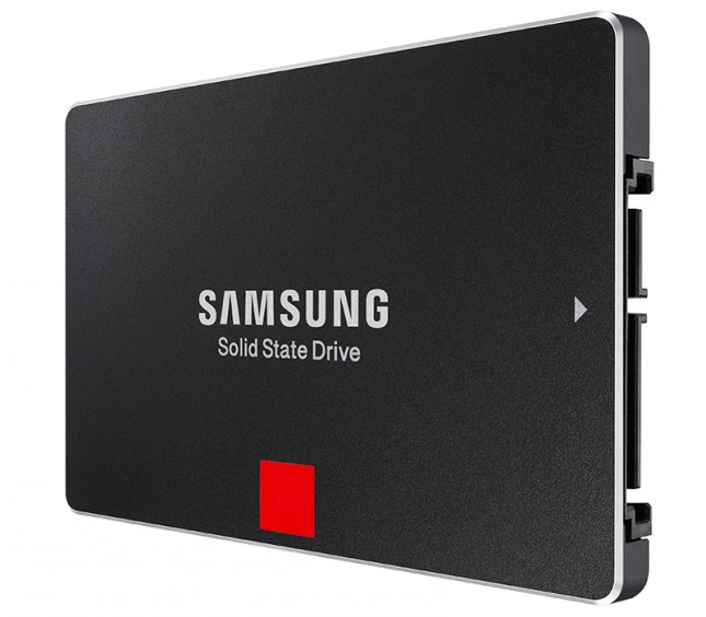
During the early days of SSDs, we saw rather quick development in capacities. The very first SSDs were undoubtedly small, generally 32GB or 64GB, but there was a need for higher capacities to make SSDs more usable in client environments. MLC NAND caused a rapid decline in prices and the capacities quickly increased to 128GB and 256GB. 512GB also came along fairly soon, but for a long while the 512GB drives cost more than a decent gaming PC with prices being over $1000.
I would argue that the 512GB drives were introduced too early - the adoption was minimal due to the absurd price. The industry learned from that and instead of pushing 1TB SSDs to the market at over $1000, it wasn't until 2013 when Crucial introduced the M500 with the 960GB model being priced reasonably at $600. Nowadays 1TB has become a common capacity in almost every OEM's lineup, which is thanks to both lower NAND prices and controllers being sophisticated enough to manage 1TB of NAND. The next milestone is obviously the multi-terabyte era, which we are entering with the release of 2TB Samsung 850 Pro and EVO models.
Breaking capacity thresholds involves work on both the NAND and the controller side. All controllers have a fixed number of die they can talk to and for modern 8-channel controllers with eight chip enablers (CEs) per channel the limit is typically 64 dies. With 128Gbit (16GB) being the common NAND die capacity today, 64 dies yields 1,024GB or 1TB (as it's often marketed). It's possible to utilize a single CE for managing more than one die (which is what e.g. Silicon Motion does to achieve 1TB with a 4-channel controller), but it adds complexity to the firmware design and there's a negative performance impact as the two dies on the same chip enabler can't be accessed simultaneously.
Increasing NAND capacity per die is one way to work around the channel/CE limitation, but it's generally not the most efficient way. First off, doubling the capacity of the die increases complexity substantially because you are effectively dealing with twice the number of transistors per die. The second drawback is reduced write performance, especially at smaller capacities, as SSDs rely heavily on parallelism for performance, so doubling the capacity per die will cut parallelism in half. That reduces the usability of the die in capacity sensitive applications such as eMMC storage, which don't have many die to begin with (as the same dies are often used in various different applications ranging from mobile to enterprise).

The new MHX controller
The real bottleneck, however, is the DRAM controller. Today's NAND mapping table designs tend to require about 1MB of DRAM per 1GB of NAND for optimal performance, so breaking the 1TB limit requires a DRAM controller capable of supporting 2GB of DRAM. From a design standpoint, implementing a beefier DRAM controller isn't a massive challenge, but it eats both die and PCB area and hence increases cost. Given how 2TB SSDs are currently a relatively small niche, embedding a DRAM controller with 2GB support for a mainstream controller isn't very economical, which is why today's client-grade SSD controller usually support up to 1GB to increase cost efficiency.
Initially the 850 EVO was supposed to carry a 2TB SKU at the time of launch, but Samsung didn't consider the volume to be high enough. As Samsung is the number one manufacturer of client SSDs and supplies millions of drives to PC OEMs, the company is not really in the business of making low volume niche products, hence the release of 2TB client SSDs was postponed in wait for lower pricing and higher demand as a result.
| Comparison of Samsung SSD Controllers | ||||
| MDX | MEX | MGX | MHX | |
| Core Architecture | ARM Cortex R4 | |||
| # of Cores | 3 | 3 | 2 | 3 |
| Core Frequency | 300MHz | 400MHz | 550MHz | 400MHz |
| Max DRAM | 1GB | 1GB | 512MB (?) | 2GB |
| DRAM Type | LPDDR2 | LPDDR2 | LPDDR2 | LPDDR3 |
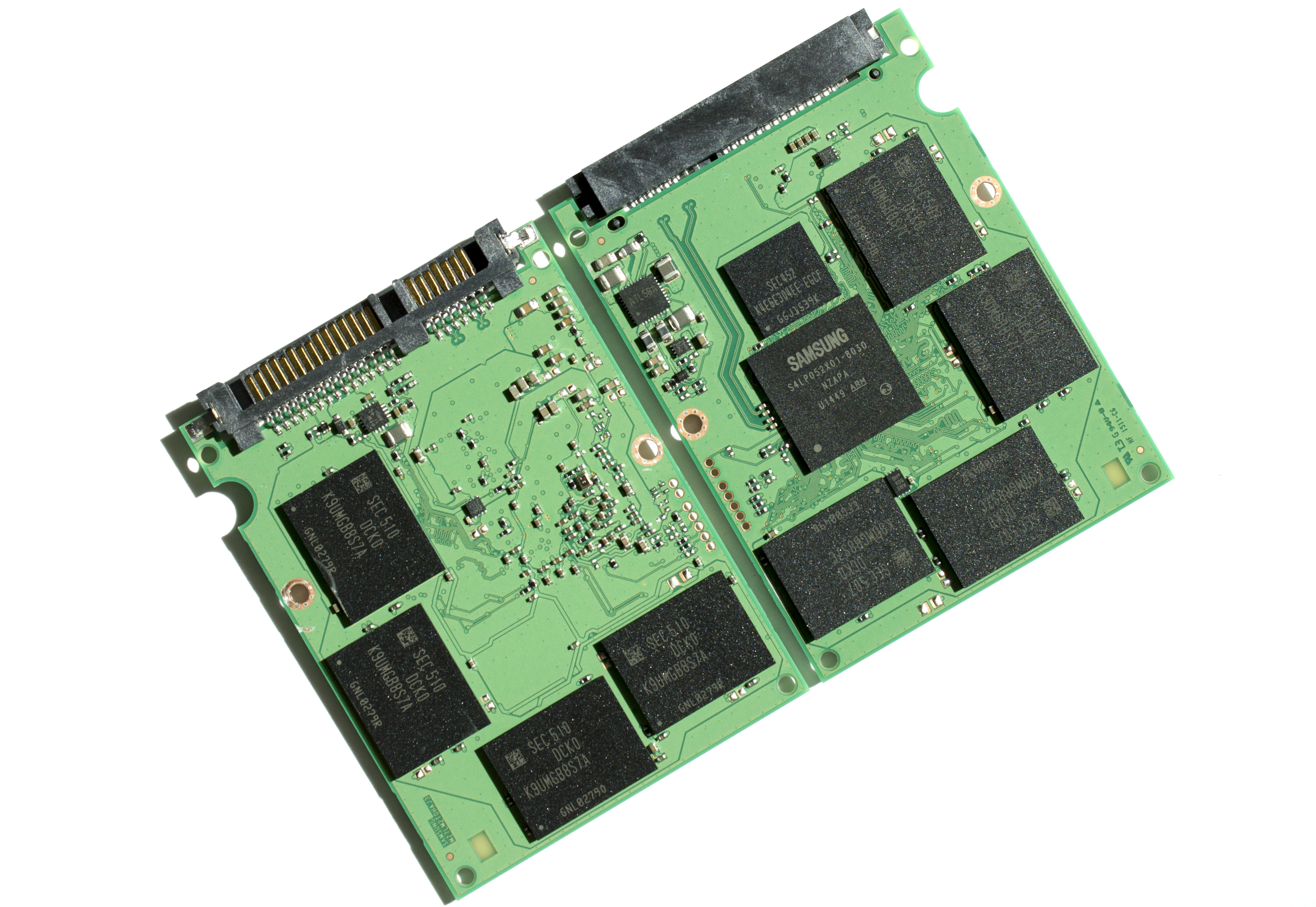
The new 2TB versions of the 850 Pro and EVO both use Samsung's new MHX controller. I was told it's otherwise identical to the MEX besides the DRAM controller supporting up to 2GB of LPDDR3, whereas the MEX only supports 1GB of LPDDR2. The MGX is the lighter version of MEX with two higher clocked cores instead of three slower ones, and it's found in the 120GB, 250GB and 500GB EVOs.
| Samsung SSD 850 Pro Specifications | |||||
| Capacity | 128GB | 256GB | 512GB | 1TB | 2TB |
| Controller | MEX | MHX | |||
| NAND | Samsung 32-layer MLC V-NAND | ||||
| NAND Die Capacity | 86Gbit | 128Gbit | |||
| DRAM | 256MB | 512MB | 512MB | 1GB | 2GB |
| Sequential Read | 550MB/s | 550MB/s | 550MB/s | 550MB/s | 550MB/s |
| Sequential Write | 470MB/s | 520MB/s | 520MB/s | 520MB/s | 520MB/s |
| 4KB Random Read | 100K IOPS | 100K IOPS | 100K IOPS | 100K IOPS | 100K IOPS |
| 4KB Random Write | 90K IOPS | 90K IOPS | 90K IOPS | 90K IOPS | 90K IOPS |
| DevSleep Power | 2mW | 5mW | |||
| Slumber Power | Max 60mW | ||||
| Active Power (Read/Write) | Max 3.3W / 3.4W | ||||
| Encryption | AES-256, TCG Opal 2.0 & IEEE-1667 (eDrive supported) | ||||
| Endurance | 150TB | 300TB | |||
| Warranty | 10 years | ||||
Specification wise the 2TB 850 Pro is almost identical to its 1TB sibling. The performance on paper is an exact match with the 2TB model drawing a bit more power in DevSleep mode, which is likely due to the additional DRAM despite LPDDR3 being more power efficient than LPDDR2. Initially the 850 Pro was rated at 150TB of write endurance across all capacities, but Samsung changed that sometime after the launch and the 512GB, 1TB and 2TB versions now carry 300TB endurance rating along with a 10-year warranty.
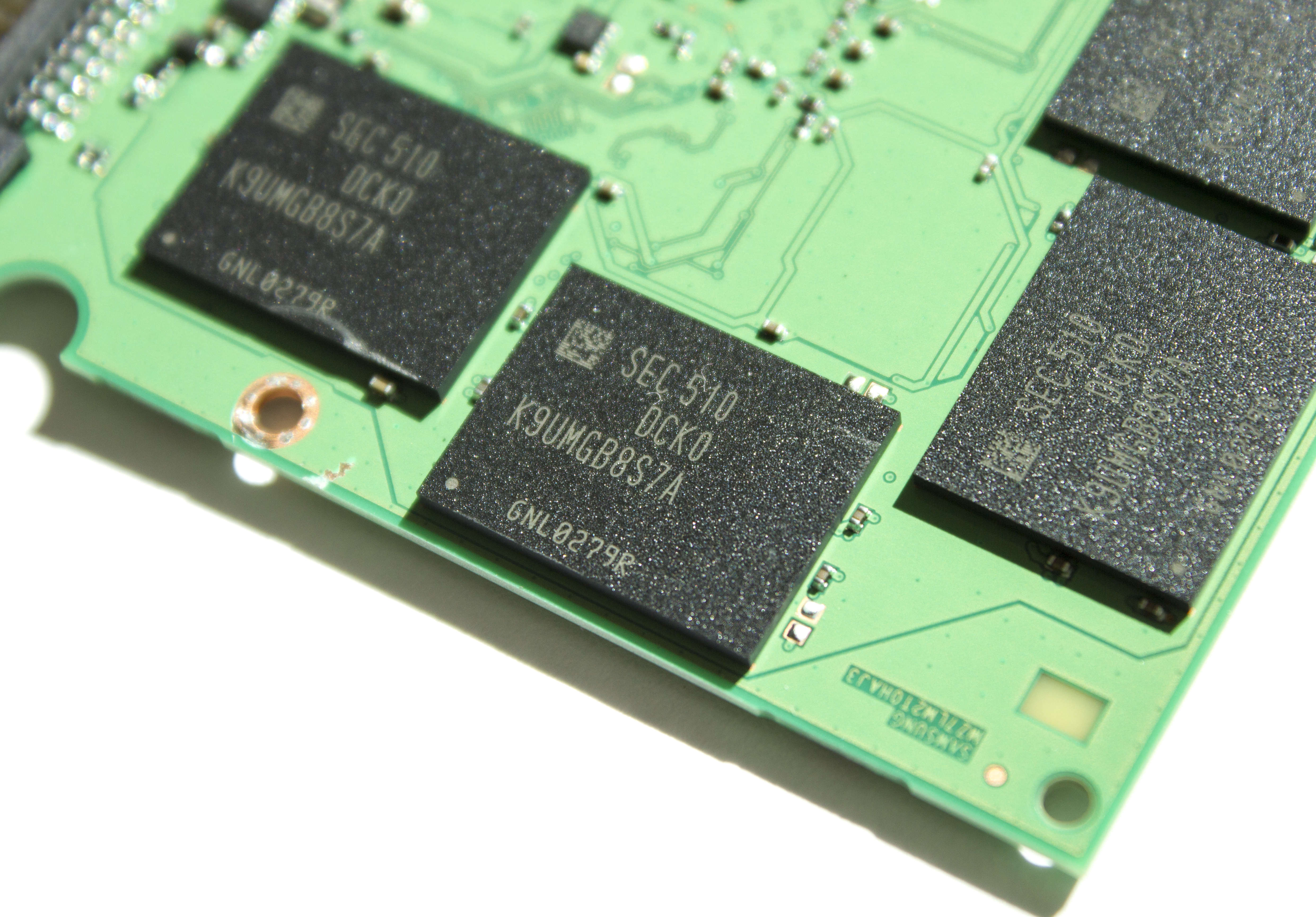
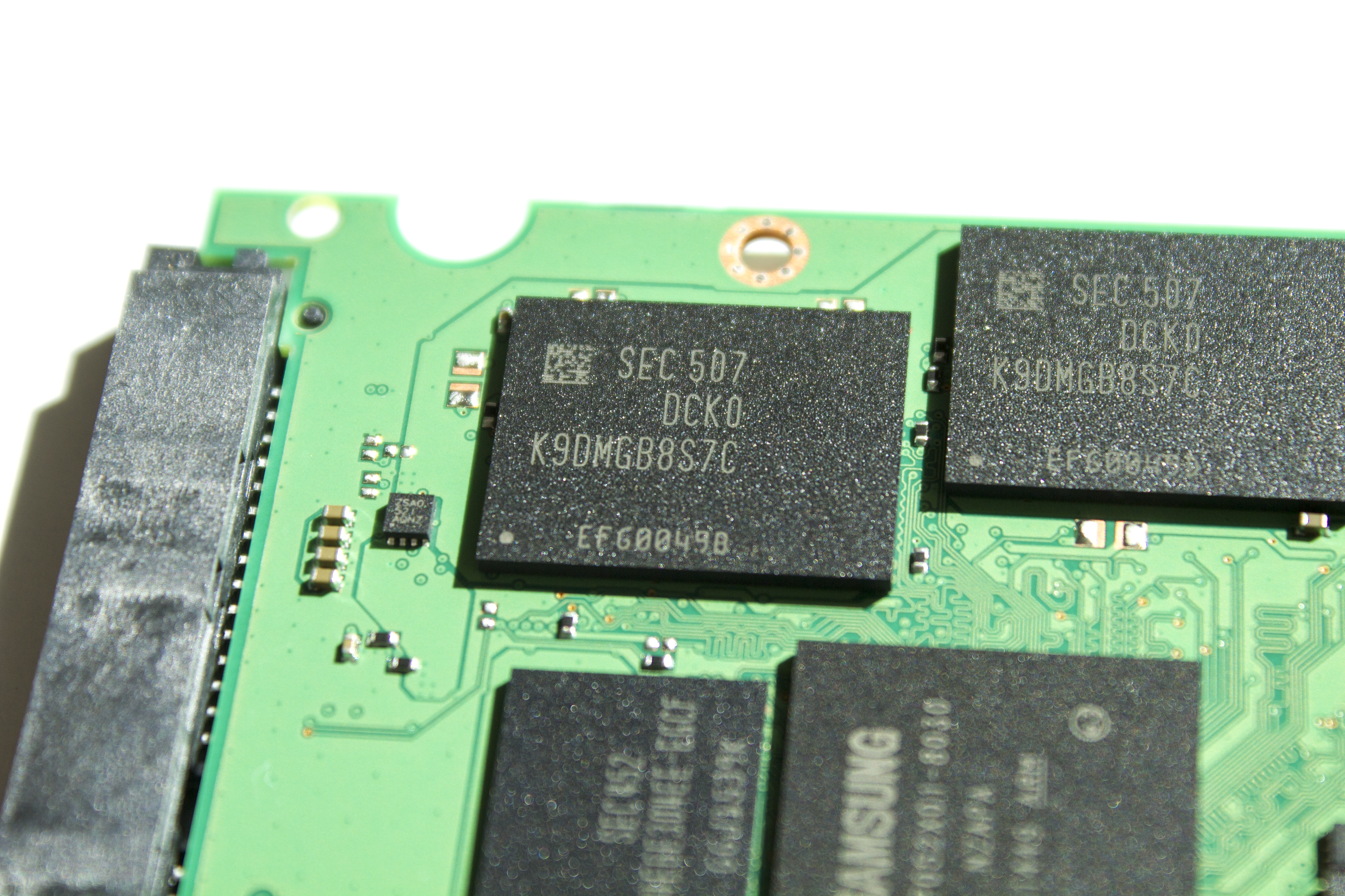
There's another hardware change in addition to the new MHX controller as the NAND part number suggests that the 2TB 850 Pro uses 128Gbit dies instead of the 86Gbit dies found in the other capacities. The third character, which is a U in this case, refers to the type of NAND (SLC, MLC or TLC) and the number of dies, and Samsung's NAND part number decoder tells us that U stands for a 16-die MLC package. With eight NAND packages on the PCB, each die must be 128Gbit (i.e. 16GiB) to achieve raw NAND capacity of 2,048GiB. 2,048GB out of that is user accessible space, resulting in standard ~7% over-provisioning due to GiB (1024^3 bytes) to GB (1000^3 bytes) translation.
According to Samsung, this is still a 32-layer die, which would imply that Samsung has simply developed a higher capacity die using the same process. It's logical that Samsung decided to go with a lower capacity die at first because it's less complex and yields better performance at smaller capacities. In turn, a larger die results in additional cost savings due to peripheral circuitry scaling, so despite still being a 32-layer part the 128Gbit die should be more economical to manufacture than its 86Gbit counterpart.
| Samsung SSD 850 EVO Specifications | ||||||
| Capacity | 120GB | 250GB | 500GB | 1TB | 2TB | |
| Controller | MGX | MEX | MHX | |||
| NAND | Samsung 32-layer 128Gbit TLC V-NAND | |||||
| DRAM | 256MB | 512MB | 1GB | 2GB | ||
| Sequential Read | 540MB/s | 540MB/s | 540MB/s | 540MB/s | 540MB/s | |
| Sequential Write | 520MB/s | 520MB/s | 520MB/s | 520MB/s | 520MB/s | |
| 4KB Random Read | 94K IOPS | 97K IOPS | 98K IOPS | 98K IOPS | 98K IOPS | |
| 4KB Random Write | 88K IOPS | 88K IOPS | 90K IOPS | 90K IOPS | 90K IOPS | |
| DevSleep Power | 2mW | 2mW | 2mW | 4mW | 5mW | |
| Slumber Power | 50mW | 60mW | ||||
| Active Power (Read/Write) | Max 3.7W / 4.4W | 3.7W / 4.7W | ||||
| Encryption | AES-256, TCG Opal 2.0, IEEE-1667 (eDrive) | |||||
| Endurance | 75TB | 150TB | ||||
| Warranty | Five years | |||||
Like the 2TB Pro, the EVO has similar performance characteristics with the 1TB model. Only power consumption is higher, but given the increase in NAND and DRAM capacities that was expected.
As the 32-layer TLC V-NAND die was 128Gbit to begin with, Samsung didn't need to develop a new higher capacity die to bring the capacity to 2TB. The EVO also uses eight 16-die packages with the only difference to Pro being TLC NAND, which is more economical to manufacture since storing three bits in one cell yields higher density than two. Out of the 2,048GiB of raw NAND, 2,000GB is user-accessible, which is 48GB less than in the 2TB 850 Pro, but the TurboWrite SLC cache eats a portion of NAND and TLC tends to require a bit more over-provisioning to keep the write amplification low for endurance reasons.
| AnandTech 2015 SSD Test System | |
| CPU | Intel Core i7-4770K running at 3.5GHz (Turbo & EIST enabled, C-states disabled) |
| Motherboard | ASUS Z97 Deluxe (BIOS 2205) |
| Chipset | Intel Z97 |
| Chipset Drivers | Intel 10.0.24+ Intel RST 13.2.4.1000 |
| Memory | Corsair Vengeance DDR3-1866 2x8GB (9-10-9-27 2T) |
| Graphics | Intel HD Graphics 4600 |
| Graphics Drivers | 15.33.8.64.3345 |
| Desktop Resolution | 1920 x 1080 |
| OS | Windows 8.1 x64 |
- Thanks to Intel for the Core i7-4770K CPU
- Thanks to ASUS for the Z97 Deluxe motherboard
- Thanks to Corsair for the Vengeance 16GB DDR3-1866 DRAM kit, RM750 power supply, Hydro H60 CPU cooler and Carbide 330R case


66 Comments
View All Comments
twizzlebizzle22 - Thursday, July 23, 2015 - link
Damn, we are in the future here. Roll in the day when my media storage drives are all SSD.Interesting as to why they managed to double the drive durability from 150TB to 300TB. That's pretty substantial.
joex4444 - Thursday, July 23, 2015 - link
Durability is the amount of data that can be written to the drive Samsung is guaranteeing can be written to it during its life. It's just related to the number of times a chip can be completely rewritten. If you double the capacity, you double the number of chips, and therefore you double the durability.lilmoe - Thursday, July 23, 2015 - link
Sure, but Samsung is also setting the older 512GB and 1TB at 300TB endurance rating up from 150TB previously, which is nice.SleepyFE - Friday, July 24, 2015 - link
If i'm not mistaken that was a marketing move. The EVO was sold as 150 so that people who needed more would buy PRO. There was a super punishing SSD test half a year back (a bit less maybe) where they tested how much the drives can take before the cells give up and even the EVO held out beyond 300. So they didn't really manage to improve anything, they just decided to extend their guarantee.leexgx - Saturday, July 25, 2015 - link
EVO not as reliable as the Pro (TLC EVO vs MLC PRO,) the pro drive never failed with bad data it silently failed at 2PBthe endurance is for warranty before where they have found errors have cropped up, the PRO drive use MLC so is reliably less error prone (as in they handle any minor errors better then TLC) then EVO under extreme loads (drives might look the same but the flash is not)
leexgx - Thursday, July 23, 2015 - link
sorry if this is been asked before, is the 25% OP been done via the ATA command that allows you to set amount of useable space or are you just partitioning it (both after a Secure erase)Samus - Thursday, July 23, 2015 - link
You don't even need to go that far. The Samsung Magician toolbox allows you to set a RAW OP "partition"leexgx - Thursday, July 23, 2015 - link
i looked online i guess it worked as i thought it would, you can use ATA LBA limit command to hard limit the OP space or just make the partition say 20GB less then the size of the SSD (or what ever size you want) this is assuming its a fresh drive or secured erased state, but the thing is TRIM does the same thing any way (assuming you don't fill the drive so it runs out of space) if you cant use TRIM then you need to set higher OP space (recommended any way)TEAMSWITCHER - Thursday, July 23, 2015 - link
Not quite yet.... I've been limping along with a pair of 840 EVO's waiting for this Samsung 3D flash in an m.2 form factor with a PCIe x4 with NVMe controller. All of this technology is mature, and my motherboard has the m.2 slot and BIOS support for NVMe, but Samsung hasn't put it all together yet. I'm not shelling out any more money for SATA III SSDs when I feel that any time now...Samsung will introduce the product I've been hoping for. Am I foolish to think this product in imminent?Impulses - Thursday, July 23, 2015 - link
Hmm, I'm not sure anyone could really say... It's plausible they might skip retail availability of the SM951 AHCI & NVMe versions altogether and release something with 3D NAND this year, but I think they haven't released the former to begin with because the demand just isn't there outside of OEMs.Might change after Skylake, might not, I doubt the average enthusiast is chomping at the bit to pay $1/GB for a drive but I dunno how much cheaper the SM951 would be in volume. I'm just aiming for a 256GB SM951 post-Skylake, for the OS, paired with 850 EVOs for storage.