Everything You Always Wanted to Know About SDRAM (Memory): But Were Afraid to Ask
by Rajinder Gill on August 15, 2010 10:59 PM ESTEvery read/write memory transaction can be segmented by type into one of three performance bins depending on the status of the bank/page to be accessed. These bins, in order of best to worst, are page-hit, page-empty, and page-miss. For the most part, anything we can do to increase the number of page-hit transactions or reduce the number of page-miss transactions is a good thing.
A page-hit access is defined as any read or write operation to an open page. That is, the bank containing the open page is already active and is immediately ready to service requests. Because the target page is already open, the nominal access latency for any memory transaction falling into this category is approximately tCAS (the CAS Latency of the device).
Click to enlarge
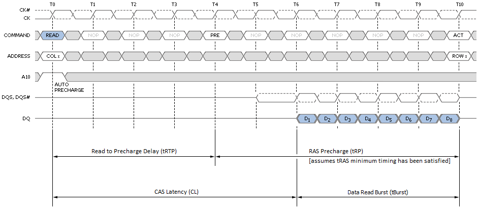
Figure 6 shows the minimum read latency associated with a best-case page-hit scenario. For a part with a CAS Latency of 6T, the memory controller waits only six short clocks before the start of data return. During a Read with Auto-Precharge, the Read command will execute as normal except the active bank will begin precharging CAS-latency (CL) clock cycles before the end of the burst. This feature allows the precharge operation to be partially or completely hidden during periods of burst read cycles, dependent on CL. When tuning our systems we always seek to set tRTP such that tRTP + tRP equals CL + tBurst for exactly this reason. Put another way, if CL and tRP are the same set 4T for DDR3 (2T for DD2).
Sequential reads to the same page make these types of transactions even more profitable as each successive access can be scheduled at a minimum of tBurst (4T) clocks from the last. The timing is captured as the CAS-to-CAS Delay (tCCD) and is commonly referred to as 'Back-to-Back CAS Delay' (B2B), as shown per Figure 7. This feature makes possible extremely high data transfer rates for total burst lengths of one page or less - in our case, 8KB.

Click to enlarge
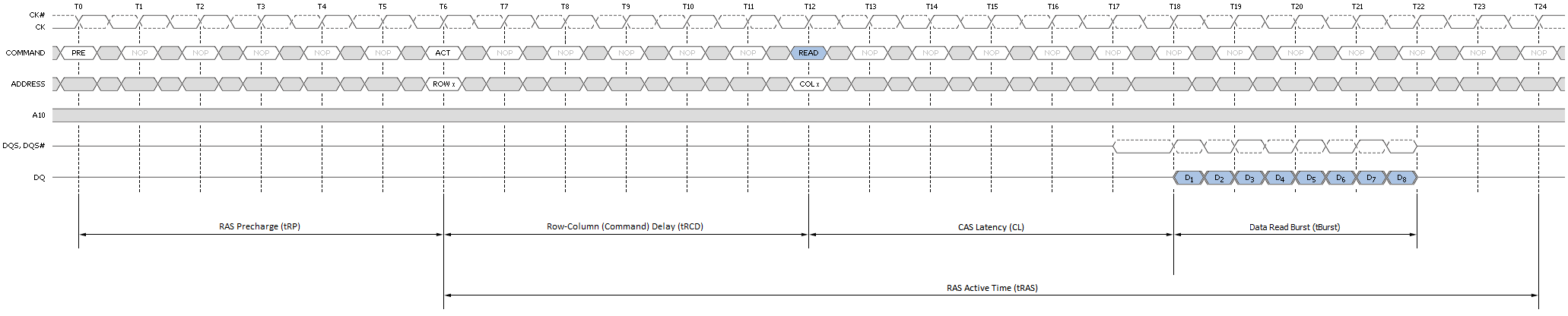
Although not ideal, a page-empty access is still preferred to a miss. In this case the bank to be accessed is Idle with no page open. Common sense tells us any attempt to read or write data to a page in this bank first requires we Activate the bank. In other words, nominal access latency now includes the time to open the page - Row-Column (or Command) Delay (tRCD). This is a doubling of the minimum access latency when compared to that of the page-hit case! Twelve cycles (tRCD + CL) now elapse before the first word is returned. Figure 8 shows this the detail.
![]()
Click to enlarge
Finally, as if the relative penalty of page-empty access wasn't bad enough, here comes page-miss. A miss occurs anytime a memory transaction must first close an open page in order to open an alternate page in the same bank. Only then can the specified data access take place. First closing an open page requires a Precharge, adding the RAS Precharge (tRP) delay to any already lengthy operation. As you can see by Figure 9, the nominal latency of an access of this type is three times that of one page-hit operation!
Click to enlarge
The relative gain/loss ratio for each access type can be quickly assessed simply through a cursory review of the most basic device timings. Imagine a memory kit rated for operation at DDR3-1600, 6-6-6-18 (CL-tRCD-tRP-tRAS): With nothing more we can estimate six cycles for a page-hit access, 12 cycles for a page-empty access, and 18 cycles for a page-miss access.
Normalized to the page-hit access latency, page-empty access is twice as long, and page-miss access is a whole three times as long. If we combine this with what we know about the inner functions of the SDRAM state machine we see page-hit and page-miss are really just subsets of the same bank state (active). Of course, page-empty access necessarily implies an idle bank. The following proof rewards us with some powerful insight.
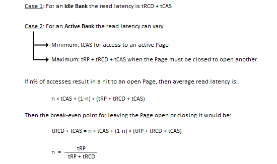
The variable n also represents the percentage of accesses to banks with open pages that must result in a page-hit access if we are to simply pace the nominal access latency that would be achieved if every read access was to an idle bank. And the only thing this depends on is the RAS Precharge delay and the Row-Column (or Command) Delay of the device in question.
You would think by working to maximize n, performance would be maximized as well. And you'd be right. Let's take what we've learned thus far and step it up a notch. We promise, after this you'll never see memory timings in the same light ever again.
Before proceeding, we've prepared a video for those of you that would like to view a few simple animations meant to help visualize each transaction type:


46 Comments
View All Comments
Dwebtron - Monday, August 16, 2010 - link
How did you know I was afraid to ask!!0ldman79 - Tuesday, May 28, 2019 - link
It's because we're all from the future.neslog - Monday, August 16, 2010 - link
Thank you for a great article on memory and you are right, I was afraid to ask.landerf - Monday, August 16, 2010 - link
I've found for the i7 platform the perfect ram setup is 1200 Mhz + cas5 or 6 timings, a 3:1 uncore ratio, and a B2B of 4. Not only does this perform well even in synthetics, it provides the "smoothest" intel experience. Something people who use amd and intel have been complaining about intel lacking. Check this chart and see how well that setup performs compared to all the conventional 2:1 setups. https://spreadsheets.google.com/ccc?key=0AsaXlcTga...Servando Silva - Monday, August 16, 2010 - link
Thanks for a great article. It will take me a while to read it carefully and fully understand it.Kris + Raju = Killer combo.
neslog - Monday, August 16, 2010 - link
On page 8 you may want to change the wording in the last paragraph " Once you've had...to cordially invite[d] (you) to do some..."
Thanks again for the article. I appreciate all the work that went into putting it together
elforeign - Monday, August 16, 2010 - link
It's a site willing to go the extra mile like this to report and educate the masses that are truly worth the time to peruse and read the posted articles. I check this site daily because there is always something interesting to read. Thank you to all the staff who do a great job here!chizow - Monday, August 16, 2010 - link
Just kidding....Or am I? :D
JarredWalton - Monday, August 16, 2010 - link
There's obviously benefits to either direction. Reducing latency is definitely a priority, but something not mentioned in the text that bears repeating is that latency is a factor of clock speed as well as the various timings. While CAS 6 will always be better than CAS 7 at the same base clock (and likewise for the other timings), if you have a faster memory speed CAS 7 could end up being better.So here's the scoop:
DDR3-1066 = 266MHz base clock, or 3.75ns per cycle.
DDR3-1333 = 333MHz base clock, or 3.00ns per cycle.
DDR3-1600 = 400MHz base clock, or 2.50ns per cycle.
DDR3-2000 = 500MHz base clock, or 2.00ns per cycle.
That gives this table in order of increasing latency, with rough pricing for 2x2GB. Based on pricing and latency, I've starred the best buys on Newegg:
CAS 6 DDR3-2000 = 12.0ns. ($180)
CAS 7 DDR3-2000 = 14.0ns. ($140)
CAS 6 DDR3-1600 = 15.0ns. ($115) ***
CAS 8 DDR3-2000 = 16.0ns. ($150)
CAS 7 DDR3-1600 = 17.5ns. ($101) ***
CAS 9 DDR3-2000 = 18.0ns. ($100) ***
CAS 6 DDR3-1333 = 18.0ns. ($100) ***
CAS 10 DDR3-2000 = 20.0ns. ($118)
CAS 8 DDR3-1600 = 20.0ns. ($85) ***
CAS 7 DDR3-1333 = 21.0ns. ($90)
CAS 9 DDR3-1600 = 22.5ns. ($92)
CAS 8 DDR3-1333 = 24.0ns. ($92)
CAS 7 DDR3-1066 = 26.3ns. ($80)
CAS 9 DDR3-1333 = 27.0ns. ($85)
CAS 8 DDR3-1066 = 30.0ns. ($93)
Notice how the total latency often comes in groups. The DDR3-1333 CL6, DDR3-1600 CL7, and DDR3-2000 CL9 are all priced around $100. If you buy any of these modules, there's a good chance (though YMMV) that you can tweak timings to run at whichever value makes you happiest. I'd probably err on the side of buying the higher speed rated modules, though, or at least grab the 1600MHz set.
Rick83 - Monday, August 16, 2010 - link
Your pricing comparison is sadly missing one important factor:Operating voltage.
I was at first surprised by the high cost of 1333/9, but I expect the voltage of that kit to be around 1.5, where most 1333/7 kits already clock in at 1.65.
The 2000/9 kit probably also runs higher V's than the identically priced 1333/6?
Lower voltages are usually preferred, as they give you a) more headroom and b) less heat at stock - with on-die controllers even less cpu heat.