Everything You Always Wanted to Know About SDRAM (Memory): But Were Afraid to Ask
by Rajinder Gill on August 15, 2010 10:59 PM ESTWhat do you mean you've never heard of Adaptive Page Management (APM) Technology? Well, that must be because Intel Marketing doesn't seem to feel the need to bring it up.
Simply put, Intel's APM determines, based on the potential implications of pending memory transactions, whether closing open pages, or allowing them to remain open longer may be beneficial to overall memory performance. In response, the memory controller may (or may not) elect to issue commands to close pages, depending on the programmed operation.
Figure 10 provides the general flow of events required to manage such a process. In our explanation we intend to introduce you to all known register settings needed to adjust the functional control policy, but first we need to detail the necessary actions, and purpose, of the design elements that make up such a mechanism. A better understanding of the underlying logic will pay dividends as you attempt to dial in measurable performance improvements through experimentation.
Per Figure 11, the Transaction Queue stores memory transactions generated by the processor. Unlike a typical First-In-First-Out (FIFO) queue with a tail, into which memory transaction may be pushed, and a head, from which memory transactions may be popped, this transaction queue is a plurality of storage elements allowing single memory transactions to be removed from the list and dispatched toward the memory in a different ordering than when originally added to the queue.
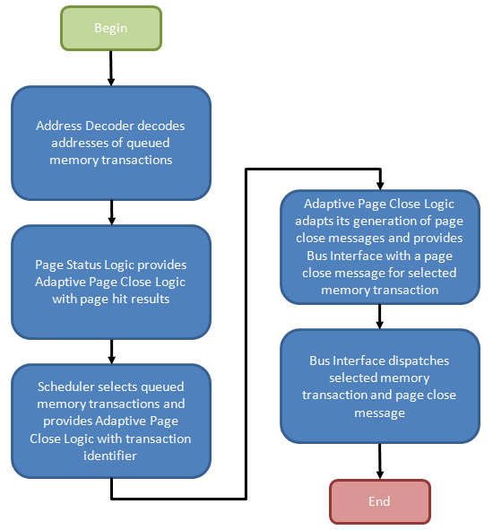
Command re-ordering can improve perceived memory performance by grouping together reads/writes to a common physical page in memory, saving the time that would otherwise be needed to later re-open the same page, should a concurrent access to the same bank force it to close early. After all, the minimum delay between sequential accesses to the same open page is equal to the CAS Latency (CL or tCAS) of the device. Accessing a bank (opening a page) increases the latency of the post-interleaved operation by the Row-Column (or Command) Delay (tRCD), approximately doubling the effective data access time.
One should also appreciate that there are varying degrees of freedom when shuffling transactions in time. Like in the case of a read and write to the same memory location: the memory controller would be disallowed from moving the dependent read either ahead of or behind the associated write as the ordering must be implicitly maintained or coherency will be lost.
The Address Decoder partially decodes the memory transactions stored in the Transaction Queue as needed to determine the bank and page selected by each queued request. From there, the Bank Select messages control the multiplexers used to input the contents of a Bank Register to a comparator used to check if the selected page was also the most recently opened page for that bank (as such, each Bank Register is large enough to store n bits where each bank comprises 2n pages). A match results in the creation of a Page-Hit Result message.
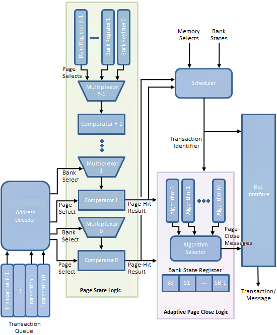
Triggered by the Page State Logic, the Scheduler fetches pre-identified queued memory transactions for re-ordering based on the Memory Selects (both bank and page) and the associated Page-Hit Results. An array of Bank State Registers track actions performed upon each bank by storing a state-word indicating, among other things, whether the Adaptive Page Close Logic decided to close the bank in response to a previous memory transaction to the same bank.
Finally, based on the policy instantiated by the Algorithm Selector, a Page-Close Message either is or is not generated based on the same Page-Hit Results, Bank State Registers, and Bank/Page Selects in an effort to increase the number of subsequent page-hit accesses and/or decrease the number of page-miss accesses.
An immediate and tangible gain is achieved for every successfully re-ordered transaction as a page-hit access is more efficient than a page-empty, or at worst, a page-miss. This is always the case with Core i7 and is one of this architecture's well known shinning points. Switch off Adaptive Page Management (disable Adaptive Page Closing in BIOS) and this is where the process ends. The page may stay open for some finite time or it may be closed right away; we're not sure as there's really no way to know without some inside help.
The Adaptive Page Close Logic must now decide whether to collect all winnings, and close the page, or let it ride, and leave it open just a while longer. While another page-hit access may yield further gains, "guessing" wrong will cause a costly page-miss access in place what would have been just a page-empty access. If only there were some way the system could measure the effectiveness of previous close decisions and then adjust policy to fit...
Surprise! The Page Manager - made up of the Page State Logic, Adaptive Page Close Logic, and Scheduler - does exactly this. How this effectiveness is measured, and how the result of that evaluation is used to adapt the decision-making process is our next topic of discussion.


46 Comments
View All Comments
Dwebtron - Monday, August 16, 2010 - link
How did you know I was afraid to ask!!0ldman79 - Tuesday, May 28, 2019 - link
It's because we're all from the future.neslog - Monday, August 16, 2010 - link
Thank you for a great article on memory and you are right, I was afraid to ask.landerf - Monday, August 16, 2010 - link
I've found for the i7 platform the perfect ram setup is 1200 Mhz + cas5 or 6 timings, a 3:1 uncore ratio, and a B2B of 4. Not only does this perform well even in synthetics, it provides the "smoothest" intel experience. Something people who use amd and intel have been complaining about intel lacking. Check this chart and see how well that setup performs compared to all the conventional 2:1 setups. https://spreadsheets.google.com/ccc?key=0AsaXlcTga...Servando Silva - Monday, August 16, 2010 - link
Thanks for a great article. It will take me a while to read it carefully and fully understand it.Kris + Raju = Killer combo.
neslog - Monday, August 16, 2010 - link
On page 8 you may want to change the wording in the last paragraph " Once you've had...to cordially invite[d] (you) to do some..."
Thanks again for the article. I appreciate all the work that went into putting it together
elforeign - Monday, August 16, 2010 - link
It's a site willing to go the extra mile like this to report and educate the masses that are truly worth the time to peruse and read the posted articles. I check this site daily because there is always something interesting to read. Thank you to all the staff who do a great job here!chizow - Monday, August 16, 2010 - link
Just kidding....Or am I? :D
JarredWalton - Monday, August 16, 2010 - link
There's obviously benefits to either direction. Reducing latency is definitely a priority, but something not mentioned in the text that bears repeating is that latency is a factor of clock speed as well as the various timings. While CAS 6 will always be better than CAS 7 at the same base clock (and likewise for the other timings), if you have a faster memory speed CAS 7 could end up being better.So here's the scoop:
DDR3-1066 = 266MHz base clock, or 3.75ns per cycle.
DDR3-1333 = 333MHz base clock, or 3.00ns per cycle.
DDR3-1600 = 400MHz base clock, or 2.50ns per cycle.
DDR3-2000 = 500MHz base clock, or 2.00ns per cycle.
That gives this table in order of increasing latency, with rough pricing for 2x2GB. Based on pricing and latency, I've starred the best buys on Newegg:
CAS 6 DDR3-2000 = 12.0ns. ($180)
CAS 7 DDR3-2000 = 14.0ns. ($140)
CAS 6 DDR3-1600 = 15.0ns. ($115) ***
CAS 8 DDR3-2000 = 16.0ns. ($150)
CAS 7 DDR3-1600 = 17.5ns. ($101) ***
CAS 9 DDR3-2000 = 18.0ns. ($100) ***
CAS 6 DDR3-1333 = 18.0ns. ($100) ***
CAS 10 DDR3-2000 = 20.0ns. ($118)
CAS 8 DDR3-1600 = 20.0ns. ($85) ***
CAS 7 DDR3-1333 = 21.0ns. ($90)
CAS 9 DDR3-1600 = 22.5ns. ($92)
CAS 8 DDR3-1333 = 24.0ns. ($92)
CAS 7 DDR3-1066 = 26.3ns. ($80)
CAS 9 DDR3-1333 = 27.0ns. ($85)
CAS 8 DDR3-1066 = 30.0ns. ($93)
Notice how the total latency often comes in groups. The DDR3-1333 CL6, DDR3-1600 CL7, and DDR3-2000 CL9 are all priced around $100. If you buy any of these modules, there's a good chance (though YMMV) that you can tweak timings to run at whichever value makes you happiest. I'd probably err on the side of buying the higher speed rated modules, though, or at least grab the 1600MHz set.
Rick83 - Monday, August 16, 2010 - link
Your pricing comparison is sadly missing one important factor:Operating voltage.
I was at first surprised by the high cost of 1333/9, but I expect the voltage of that kit to be around 1.5, where most 1333/7 kits already clock in at 1.65.
The 2000/9 kit probably also runs higher V's than the identically priced 1333/6?
Lower voltages are usually preferred, as they give you a) more headroom and b) less heat at stock - with on-die controllers even less cpu heat.