Intel Shows Off Work on Next-Gen Glass Core Substrates, Plans Deployment Later in Decade
by Ryan Smith on September 18, 2023 9:01 AM EST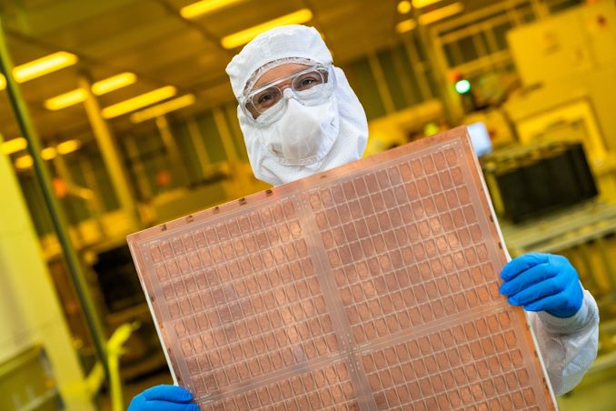
Although Intel’s annual Innovation event doesn’t kick off until tomorrow, the company is already publishing some announcements ahead of the show – and it’s not the trivial stuff, either. This morning the company is showing off their initial work on developing a glass core substrate and associated packaging process for their chips. As a result of their progress with research and development on the glass cores, Intel is now planning on introducing glass core substrates to its products in the second half of this decade, allowing them to package chips in more complex, and ultimately higher-performing configurations.
There’s a lot to unpack from Intel’s relatively short announcement, but at a high level, glass core substrates have been under research across the industry for over a decade as a replacement for organic substrates, which are widely used in current-generation processors. Essentially the medium that typical silicon dies sit on, substrates play an important part in chip packaging. First and foremost, they provide the structural stability for a chip (silicon dies are quite fragile and flimsy), and they are also the means through which signals from silicon dies are carried, either to other on-package dies (i.e. chiplets), or to the large number of relatively sizable pins/pads on the back side of a chip. And, as chip sizes have increased over the years – and the number of pins/signals required by high-end chips has, as well – so has the need for newer and better materials to use as a substrate, which is what’s been driving Intel’s latest accomplishment.
Ultimately, what Intel is aiming to do with glass core substrates is to improve upon what can be done with existing organic substrates, allowing for larger chips with more signals to be routed through the substrate more cleanly. And while this will potentially have benefits for all chips over a long enough time, the immediate focus is on high-end, multi-chiplet processors, where glass core substrates will offer better mechanical stability, better signal integrity, and the ability to more easily route a larger number of signals through a non-silicon medium. In short, Intel considers it one of the keys to making high-performance processors in the next decade.
Substrates: A Quick Recap
The need for substrates goes back to some of the earliest days for large-scale integrated chips, where chip designs reached thousands and tens of thousands of transistors. These small transistors needed to be wired to much larger pins in order to be installed in systems by relatively massive human hands, leading up to the first chip packages, such as dual in-line packages. These used a frame – typically a lead frame – to hold the actual silicon die, with the frame (or alternatively, wire bonds) providing the signal paths between the die and external pins.
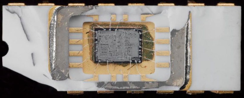
Intel 4004 Delidded (Image Courtesy Science Museum Group Collection Online - CC BY-SA 4.0)
Since the 70s, there have been several evolutions in substrate designed. Metal frames gave way to classic ceramic chip in the 90s, and then organic packaging around the turn of the millennium. Each iteration of substrate had better properties than the last, above all else, making it easier to route a larger number of signal and power pins to increasingly complex dies.
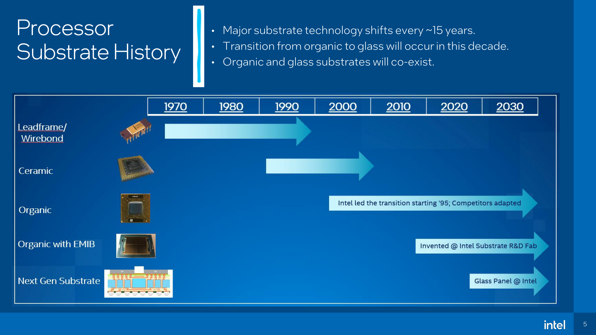
While you’ll still find lead frame and ceramic chips here and there, organic substrates have been the bread and butter of the industry for the last couple of decades. The organic material, essentially made of PCB-like material layered with woven glass laminates, allows for a fairly large number of signals to be routed through a chip, including basic chiplet designs such as Intel’s mobile processors (with PCH separate PCH and CPU dies) as well as AMD’s chiplet-based Zen processors.
But organic substrates have already been a limiting factor for some time now, especially in high-end chips. Which is why over the last decade we’ve seen the rise of ultra-high-density interconnect interfaces such as silicon interposers (chip on wafer on substrate), and their derivatives like Intel’s own EMIB. These have allowed companies to bridge together the critical paths of their chips with fast and dense pieces of silicon, but at fairly high costs, and without entirely resolving the drawbacks of organic substrates. As a result, Intel has also been searching for a true replacement for organic substrates, one that will play nicely with large chips, and while not replacing the need for CoWoS/EMIB at the highest level, would offer better signal performance and denser routing than organic substrates today.
Glass Core Substrates: Finer, Yet Stronger
This brings us to the topic of today’s announcement from Intel, glass core substrates. The company has been working on replacing organic substrates with glass for over a decade now, and they’ve finally reached the point of progress where they’re ready to show it off to the world while planning for its use in future products.
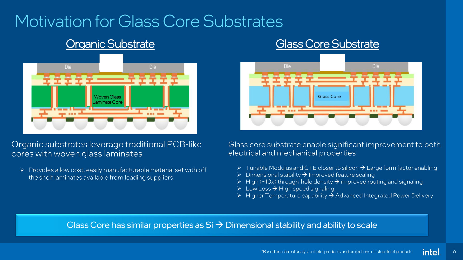
At a high level, a glass core substrate is just that: replacing the organic, PCB-like material of an organic package with glass. To be sure, this doesn’t mean replacing the entire substrate with glass – so Intel is not going to be mounting chips on pure pieces of glass – but rather, the material at the core of the substrate would be made of glass. Meanwhile, metal redistribution layers (RDLs) would still be present on both sides of a chip, providing the actual pathways between various pads and solder joints.
Glass Core Substrates In Panel Form
While harder to work with than the now well-established organic substrate, Intel considers glass substrates to be superior both in mechanical and electrical properties, which in turn makes them desirable to use in future chips. Or, conversely, less undesirable than organic substrates when building very large chips.
Starting from the mechanical side of matter, Intel reports that glass core substrates offer far better mechanical strength than organic substrates. They’re able to withstand higher temperatures better than organic substrates during packaging, resulting in less warping and distortion. Glass is also reportedly easier to get flatter as well, which makes packaging and lithography easier. Finally, glass has a similar coefficient of thermal expansion as silicon (unlike organic substrates), meaning that what little warping that still occurs from heat is consistent with the dies above, as opposed to having different parts of a chip expanding at different rates.
Most importantly, perhaps, is that all of those items taken together open the door to producing larger chips. With a more stable substrate to mount the dies on, it will be possible to have larger dies and a larger number of dies all sharing a single substrate – and thus behaving as a single chip.
Bridging the gap between mechanical and electrical, according to Intel, they’re also able to achieve a much tighter pitch on the through-glass vias (TGVs) that carry signals through the substrate itself, allowing for a much larger number of vias overall. Intel is reporting that they’re able to space TGVs less than 100 microns (µm) apart, allowing for a 10-fold improvement in TGV density. All of which ultimately allows for more flexibility in routing signals through the substrate core, and to some extent makes it easier to route signals with fewer RDL layers.
Assembled Test Chip Substrates
All of this, in turn, allows for not only larger chips, but for more dies to be placed on a same-sized chip. According to Intel, glass packaging would allow them to place 50% more dies on a chip – or rather, the die complex area within a chip could be 50% larger – allowing for more densely packed chips than what Intel can do today.
Finally, on the electrical side of matters, glass core substrates, and more specifically the TGVs, reportedly offer better electrical performance as well. Owing to the low loss nature of the dielectric used in TGVs combined with the much larger number of them, Intel says that glass core substrates will allow for cleaner signal routing and power delivery. In the case of the former, that means being able to do 448G signaling through copper, rather than having to use optical interconnects. Meanwhile, lower-loss power delivery would improve overall chip efficiency by that much more, by reducing the amount of energy that is lost as heat before it even reaches the processor dies.
Farther down the line still, glass core substrates should also make co-packaged optics easier to accomplish for when you do want to use optical. A glass substrate would allow for optical interconnects to be integrated right into the chip, rather than having to tack it on in other manners.
So if glass is so great, what’s the catch? While Intel is understandably more excited to talk about what’s good about glass core substrates and what they’ve found works well thus far, one inescapable element will be cost. Like any new technology, glass core substrates will be more expensive to produce and package with than tried and true (and cheap) organic substrates. And while Intel isn’t talking about yields this far out, it will be hard for glass to compete with organic, at least at first.
More broadly speaking, glass core substrates also means that Intel needs to bootstrap a complete ecosystem for the material. They aren’t vertically integrated with organic substrates today, and they won’t be vertically integrated with glass, either. To that end, Intel is already working with partners today to develop the necessary tooling and supply capacity, to bring themselves to initial commercial production. But over the longer-term, Intel will need to figure out how to make outsourced testing and assembly possible, especially as Intel plans to offer glass core substrates to IFS customers in the future.
Finally, it bears noting that while glass core substrates allow for a tighter signal pitch than organic substrates, they are not a replacement for EMIB, Foveros, or other more advanced packing techniques based around using silicon mediums. A 75µm pitch for a TGV is still a far cry from the 45µm pitch of EMIB, never mind the <10µm pitch planned for Foveros Direct. So all of those packaging technologies will remain complementary add-ons to glass core substrates, at best replacing EMIB in fringe cases of products that don’t need the full density improvements of EMIB.
Glass In Action: Intel’s Fully Functional Test Chip
The final part of today’s announcement from Intel is based around the manufacturing side of matters. As noted earlier, Intel has been working on glass core substrates for over 10 years now, and more recently has been embarking on a three-and-a-half-year pathfinding project to bring glass core substrates to the next step. Backing those efforts, at this point the company has a fully integrated R&D line up and running in one of their Chandler, Arizona fabs (the same one that does EMIB). Altogether, Intel has spent over a billion dollars on glass core R&D thus far.
The first fruit of their R&D efforts, Intel has completed the assembly of a set of test vehicles – multi-chip packages built over a glass substrate. The chips, which look similar to Intel’s ultra-low power mobile chips (Alder Lake-U 9W?), are reportedly fully functional, giving Intel some practical results to report on. While we don’t have a ton of details on the chip, Intel has told us that it uses 3 layers of RDL, and the TGVs have a pitch of 75µm.
Along with proving the electrical properties of glass, the small test chip is also intended to prove some of the physical properties, as well. The glass core was made very thick – on the order of 1mm – in order to prove that TGVs would work with such a thick core. For the kind of massive, high-end chips Intel is planning on using glass core packing for, those chips will require a very thick core in order to hit their size goals, so Intel needed to prove that TGVs would (still) work at such lengths.
Intel Glass Core Substrates: Coming Later This Decade
Wrapping things up, today’s announcement serves as a kick-off of sorts for Intel’s glass core substrate era. Following on their decade of R&D work and their pathfinding sprint, Intel now believes they are ready to begin planning for the transition to glass core substrates in their products – albeit a transition that is still several years out.
If Intel’s product development goes according to plan, the company intends to begin shipping glass core products later this decade. The first products to get the glass core substrate treatment would be their largest and most profitable products, such as high-end HPC and AI chips. These are the products most strained by the use of organic substrates today due to the size limits those substrates impose, and those are the limits intel believes would most benefit from glass core packaging.
Longer-term, the plan is to waterfall down the technology from HPC chips into smaller and smaller chips, until the technology is available (and viable) for Intel’s rank and file consumer chips. The company is very quick to note that glass and organic substrates will co-exist for years to come – and, like past transitions, there will likely still be chips using organic substrates well after glass is introduced – but the company is also optimistic that they’ll be able to bring the costs of glass core substrates down to parity with organic substrates, eventually making it possible to reap the benefits even in lower-priced processors.
And Intel won’t be keeping the technology to themselves, either. As part of the company’s broader initiative to become a world class contract foundry, Intel will be offering glass core substrates to IFS customers in due time. While it’s far too early to guess when that would be (even Intel products may be 6 years out), being able to offer glass packaging could give Intel a big leg up over its competitors, especially for producing high-end, highly-profitable chips.
Above all else, it needs to be reiterated that there’s a great deal of work Intel still needs to do in order to bring glass core substrates to the market. But if the company is successful, then the switch to glass will usher in the kind of major technology transition that only happens every 15 to 20 years.


16 Comments
View All Comments
FWhitTrampoline - Monday, September 18, 2023 - link
Maybe call that a Glass Interposer instead as that's what that in fact is! So the Traces density on Glass as opposed to Organic Substrate(PCB like material).edzieba - Tuesday, September 19, 2023 - link
It's not an interpose. The wafer is integrated onto the substrate in the same way as any other flip-chip process, not in the wafer-to-wafer bonding of a Si interposer.xol - Monday, September 18, 2023 - link
Suprised no mention of Silicon Nitride which has all the good properties of glass, plus even closer thermal expansion coefficient to silicon, AND excellent thermal conductivity.Kamen Rider Blade - Monday, September 18, 2023 - link
Interesting, how far along is Silicon Nitride as a PCB substrate?xol - Tuesday, September 19, 2023 - link
i dunno.. but as a material it's in common use in semiconductor processes, so...Starfishprime79 - Tuesday, September 19, 2023 - link
SiN has poor electrical properties, specifically very high Dk. Why glass is superior.Kevinlangford - Monday, September 18, 2023 - link
couple more tubes of thermal paste should do the trick!Dante Verizon - Monday, September 18, 2023 - link
Intel has become a company of promises, I tend not to believe anything they announce that they will achieve in the future.name99 - Monday, September 18, 2023 - link
Your annual reminder that when Intel announces a tech, it does NOT mean that Intel is the only company with that tech, or even first with that tech; just that Intel has the loudest megaphone.Other companies are also working on glass substrates and (assuming the Japanese translation is accurate...) https://eetimes.itmedia.co.jp/ee/articles/2210/25/... Apple is already using a version as the substrate for the A16.
edzieba - Tuesday, September 19, 2023 - link
That's just Apple's marketing department at work. "Epoxy glass substrate " is the organic substrate everyone has been using for decades.