Intel Unveils Meteor Lake Architecture: Intel 4 Heralds the Disaggregated Future of Mobile CPUs
by Gavin Bonshor on September 19, 2023 11:35 AM ESTIntel Meteor Lake: Changing The Strategy, Laying the Foundation for Intel 3
The strategy for both the Intel 4 process and the first architecture built on it, Meteor Lake, looks to change the dynamic for the mobile market and the foreseeable future of Intel's client processors. With the Foveros 3D packaging, opting for a power-conscious mobile platform seemed the best way to showcase their gains in terms of power efficiency.
One of the main product assembly advantages of Foveros packaging is that Intel can chop and change tiles depending on the processor, which includes current technologies, I/O, graphics, and compute cores. This approach to 3D tiled packaging also means that it is theoretically easier to introduce new tiles with faster cores with higher IPC performance, new graphics processors, and newer I/O, such as Wi-Fi 7. With Foveros not limiting Intel to use a single, monolithic die, it allows Intel to use different manufacturing processes for each of the tiles and integrate them onto the silicon. This is prevalent with the compute tile being built on Intel 4, while the graphics tile in Meteor Lake is made using TSMC's N5 node. This flexibility is key to advancing innovation, customizability, and, of course, wafer yield.
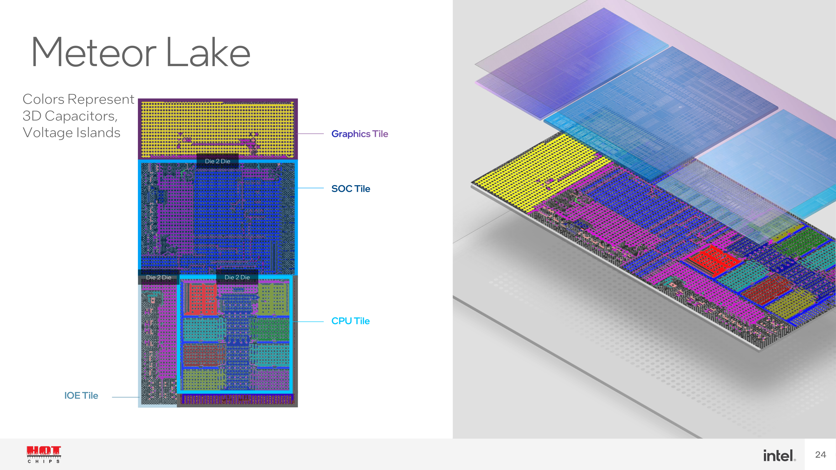
Intel Meteor Lake from Hot Chips Slide Deck
Intel also introduced a dedicated in-silicon AI engine through the NPU within the SoC tile. Similar to AMD with their Ryzen AI technology, Intel is looking to capitalize on the AI rush within its client-focused processors, but with support for OpenVINO and also including MCDM driver-compliance, users can do some pretty cool things with AI inferencing on the chip. Although these implementations aren't akin to the types of AI inferencing done in the cloud via ChatGPT with dedicated AI hardware, it's a step in the right direction in a world that looks to be slowly taken over by AI.
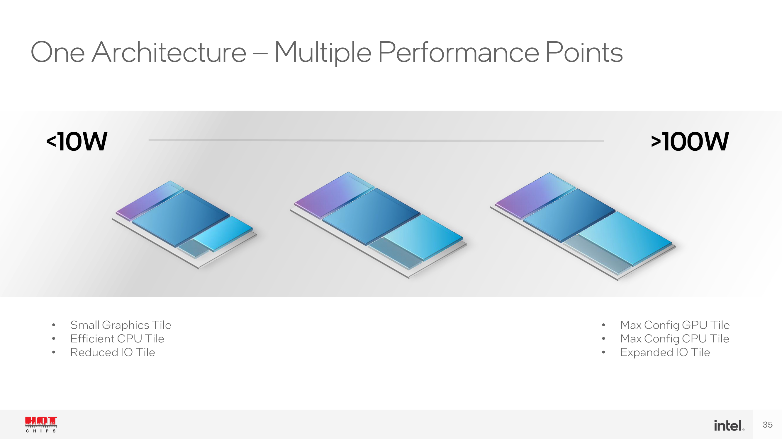
Wrapping things up, while Intel is confirming that Meteor Lake is coming to mobile-first, any details beyond that are slim pickings. At this point in time, Intel hasn't revealed anything in regard to SKUs or possible configurations. Everything disclosed is based on the 'full; Meteor Lake processors, but Intel hasn't spoken about different configurations or what the lower-end segment might look like regarding tiles and implementations. From their Hot Chips disclosures, offering a tiled architecture allows them to scale upwards and down depending on the SKU. The high-end SKU, which hasn't been disclosed yet, will feature the full configuration and implementation of all the features. Otherwise, the scalable nature of Meteor Lake and disaggregation allows for different levels of compute and graphics tiles and the ability to scale the input and output (I/O) depending on the device.
Meteor Lake will also be the first mobile platform from Intel to use their new Core naming scheme for products, which drops the 'i' from the Core branding. This includes the Core 3, 5, and 7, as well as higher spec Ultra 5, 7, and 9 Ultra tiers. Pat Gelsinger, Intel's Chief Executive Officer (CEO), during his opening keynote at Intel Innovation 2023, states that Intel is launching the first Meteor Lake Ultra (high-end) SKU with AI capabilities (NPU) on December 14th.

A tray of Meteor Lake Core Ultra processors (Credit, Intel)
We expect Intel to disclose more about specific SKUs and other specifications, such as clock speeds and core configurations, as we get closer to Meteor Lake's launch. Although we're expecting Ultra-focused Meteor Lake SKUs to launch on December 14th, no details on when we can expect other SKUs are set to hit retail channels. Meteor Lake is likely to launch with the top Ultra SKU or at least one that is close to the top of the stack.
Reading the tea leaves ahead of Innovation 2023, one gets the impression that Intel was hoping to be just a bit closer to launch by now than they actually are. But all things will eventually come in due time...


107 Comments
View All Comments
erinadreno - Tuesday, September 19, 2023 - link
Chiplets on mobile processors doesn't sound exactly enticing. Why does Intel feel the need to use 3 different types of chiplets from 2 foundries on a power-sensitive mobile chip?jazzysoggy - Tuesday, September 19, 2023 - link
It's not the same chiplet strategy as AMD is using for Zen, it's more inline with AMD's MI accelerators. Not as cheap as the Zen strategy, but much more power efficient for power sensitive mobile chips.schujj07 - Tuesday, September 19, 2023 - link
Do you have proof it is more power efficient? Intel right now is vastly less power efficient than AMD and that is regardless of chiplet or monolithic dies.Unashamed_unoriginal_username_x86 - Tuesday, September 19, 2023 - link
First page says .15-.3 pJ/bit for Foveros, AMD has previously stated infinity fabric uses "<2 pJ/bit" which presumably isn't very far under 2. this puts Intel at 5-10x the efficiency for this very specific part of data transmissionduploxxx - Wednesday, September 20, 2023 - link
first generations of infinity fabric were also less power hungry, untill they noticed what is needed to get things faster and there you go. Lots of bandwidth changes and infinity fabric changes and as well the power usage... lets see what Intel is capable of doing first, it's marketing all over the place...Samus - Tuesday, September 19, 2023 - link
Intel is behind AMD on power efficiency purely due to process node. Architecturally they are quite competitive. This is proven in how AMD performance scales when underclocked compared to Intel.Anandtech recently did an investigation into this and came to the conclusion that while the architectures are vastly different they have potentially similar performance once you determine the ideal wattage for the chip, and at the moment Intel is pushing high TDP into extremely inefficient territory to have something competitive with AMD, due to AMD being on a superior node. Basically AMD can deliver X performance at 56w while Intel can deliver X performance at 72w, but Intel can deliver Y performance at 100w while AMD delivers Y performance at 95w.
While impossible to absolutely prove, various factors can help determine this differential has more to do with manufacturing superiority than design superiority.
Intel going for tiles here is a clear attempt to close the gap on this.
PeachNCream - Thursday, September 21, 2023 - link
I think I'd second-guess anything Anandtech does these days. They had one person with an advanced degree that departed years ago after being bought out by Qualcomm when they owned Killer NICs and have since had trouble publishing articles without obvious typos and "in-a-hurry" oversights.On the other hand, if that data is supported by a more credible publisher that has decent measuring equipment and can afford to purchase its own test hardware rather than relying solely on free samples - well then we should sit up and take notice. At this point though, an Anandtech exclusive is just a reason to raise the citation needed flag and THEN further analyze the sources for their motives.
RedGreenBlue - Sunday, October 1, 2023 - link
They’ve always had typos that slip through, or grammar mistakes. All the way back to Anand’s time. I don’t like it but I know what was intended when I see one. There still isn’t another website with the same focus on the segments they focus on. I miss the deep-dives into mobile chips and phones they used to do by investigating what wasn’t publicly released about things but for most people that’s a niche purpose that other sites cover extensively with reviews and can focus on and is a bit too consumer focused and easily found elsewhere. Not really their target market.Composite - Thursday, September 28, 2023 - link
This is indeed similar to MI250 2.5D fabric. However, MI300X is full 3D fabric.elmagio - Tuesday, September 19, 2023 - link
My personal guess, from the moment this was announced, has been that they want every single cm² of silicon going through their Intel 4/EUV capacity going to the compute tile. They're lagging quite a bit behind TSMC and Samsung in terms of EUV capacity, so anything that doesn't stand to benefit much from being designed from the ground up to be made on their own nodes is worth offloading to TSMC.SoC and IO tiles are really not process-limited currently, and their Arc GPUs are in general going manufactured elsewhere anyway. But their CPU design process has always been fully in house every step of the way, and they don't want to change that (at least not yet). So everything but compute would be "wasted" Intel 4 capacity.