Intel Unveils Meteor Lake Architecture: Intel 4 Heralds the Disaggregated Future of Mobile CPUs
by Gavin Bonshor on September 19, 2023 11:35 AM ESTGraphics Tile: A Generational Leap Through Arc, Xe-LPG Graphics
As part of their disaggregated architecture for Meteor Lake, Intel has opted to use a separate tile for graphics. Intel has gone down an interesting route for its disaggregated graphics, with the most notable inclusion through an upgrade to Intel's Arc Graphics architecture. Powering Intel's integrated graphics for Meteor Lake is a new graphics architecture which Intel calls Xe-LPG (and no, we're not talking about fuel here). Based on Intel's current discrete graphics architecture known as Xe-HPG (used in their Arc GPUs), Intel claims 2x performance per watt compared to the Xe-LP architecture-based Iris Xe integrated graphics within Intel's 12th Gen Core series.
There are a number of different elements within the graphics and media area of Meteor Lake, the bulk of which is built into the graphics tile, where the Xe-LPG graphics architecture is located. Unlike the compute tile (Intel 4) and the SoC tile, which is manufactured on TSMC N6 (6 nm), the graphics tile is made on TSMC's N5 node (5 nm), the same generational family as the nodes used by AMD and NVIDIA's discrete and integrated GPUs.
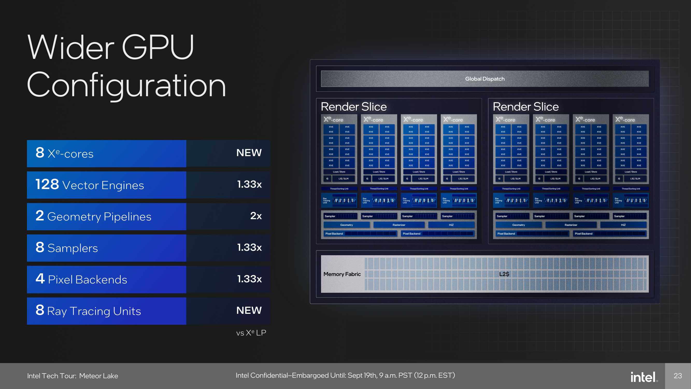
With Meteor Lake and the graphics tile with the Xe-LPG graphics processor, Intel is promising discrete-level performance in an integrated form factor. Looking at the finer specifications, Intel includes 8 x Xe graphics cores with 128 vector engines (12 per Xe core) and 8 samplers, representing a 1.33 x increase over Intel's previous Xe LP graphics. There are also 4 Pixel backends, which is an improvement over the 3 PBs on Xe LP. Intel also doubles the number of geometry pipelines within Xe-LPG, with two, and they also introduce 8 dedicated Ray Tracing Units (RTU), which is new for Intel's integrated graphics line-up.
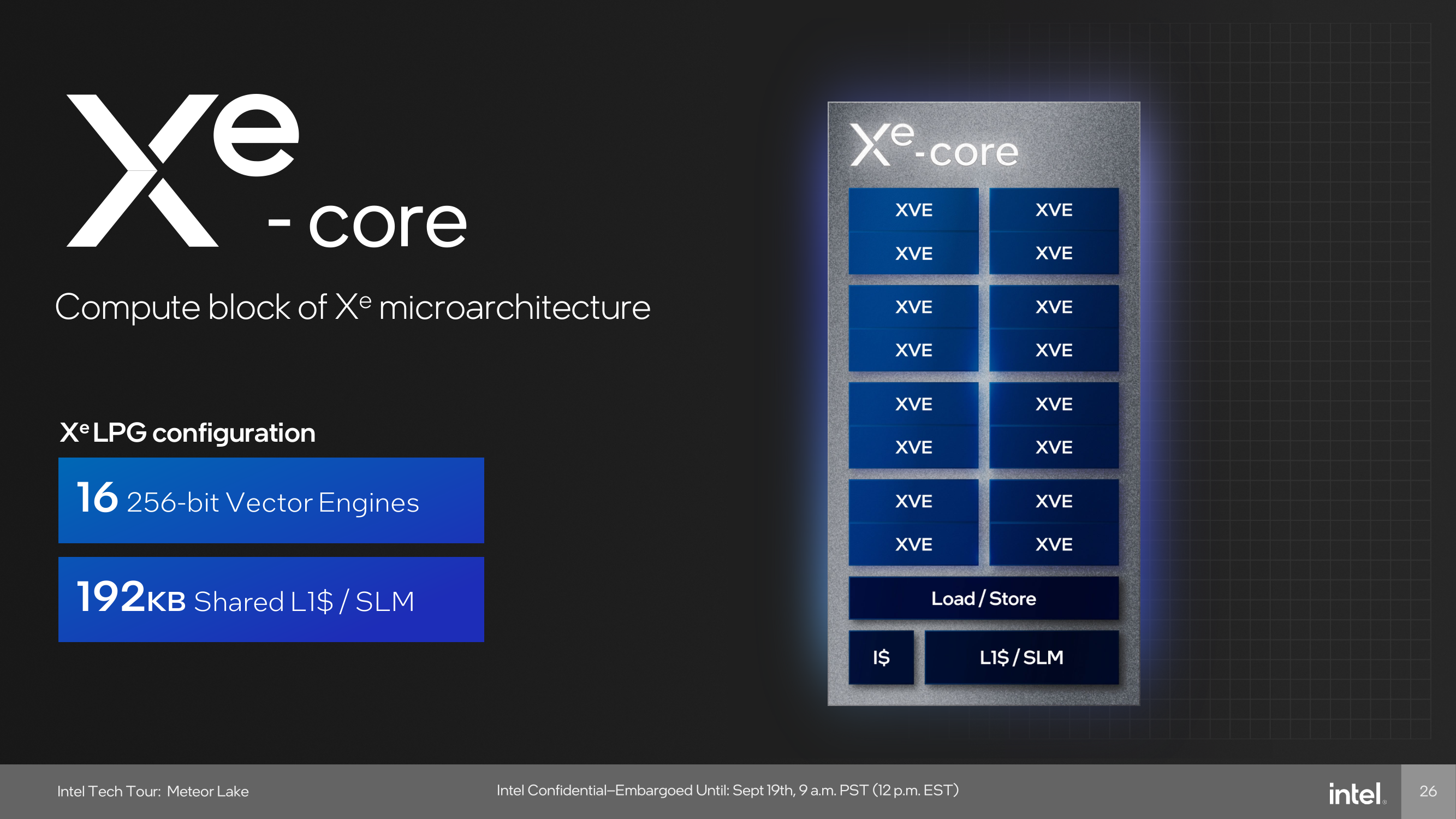
Looking at the makeup of Intel's Xe core, as previously mentioned, there are 16 Vector Engines that have a bus width of 256-bit, while each core also has 192 KB of shared L1 cache. Each Vector Engine enables 16 FP32 ops per clock, and 32 FP16 ops per clock, with a shared FP64 execution port with 64 INT8 ops per clock. One dedicated FP64 ops per clock unit is new over what's previously been seen in Raptor Lake and shares the overall design philosophy of Meteor Lake on power efficiency; pairs of Vector Engines can run in lockstep for better efficiency.
As part of Intel's goal of advancing the overall experience with Xe-LPG for users, the graphics are DX12 optimized, and Intel now brings Out of Order Samplng (OoOS) to Xe-LPG. It's worth noting that when talking about Execution Units (EUs), Intel's new and current term for this is Xe Vector Engines, or XVE for short. Intel hasn't provided us with how OoOS works within Xe-LPG, but we've reached out for more details.
| Comparing Intel Xe Integrated Graphics (Mobile) | ||||
| Meteor Lake (Xe-LPG) |
Raptor Lake (Xe-LP) |
Alder Lake GT1 (Xe-LP) |
Tiger Lake GT2 (Xe-LP) |
|
| Process Node | TSMC N5 | Intel 7 | Intel 7 | Intel 7 |
| Vector Engines/EUs | 128 | 96 | 96 | 96 |
| ALUs/Shaders | 1024 | 768 | 768 | 768 |
| TMUs | ?* | 48 | 16 | 48 |
| ROPs | ?* | 24 | 8 | 24 |
| Ray Tracing Units | 8 | - | - | - |
| TDP | ? | 15 W | 15 W | 15 W |
*Intel hasn't given us a deep dive into the finer specifications of Xe-LPG integrated graphics. Looking at an existing integrated Intel Arc equivalent with similar specs, the Meteor Lake Xe LPG could have 64 TMUs and 32 ROPs per the Arc A370M, which also has 1024 ALUs.
Comparing Intel's integrated Xe graphics from previous mobile architectures, Meteor Lake, through the Xe-LPG Arc based graphics, has 128 XVEs, which is an increase of 1.33 X or 32 XVE/EUs, than the previous Xe-LP generation. Regarding arithmetic logic units (ALUs), which are essentially shader cores, Xe-LPG has been increased to 1024, which is 128 ALUs per Xe-LPG core. As previously mentioned, Intel hasn't given us more about the finer specifications, including TMUs or ROPs, but does bring 8 Ray Tracing units, which is new for Xe-LPG when compared directly to Xe-LP.
Meanwhile, with Intel's Foveros 3D packaging technology, disaggregating the Media Engine and Display Engine from the graphics tile means when doing encoding or decoding, as well as video playback, it doesn't require the graphics tile to be powered up to do workloads on more power consuming cores.
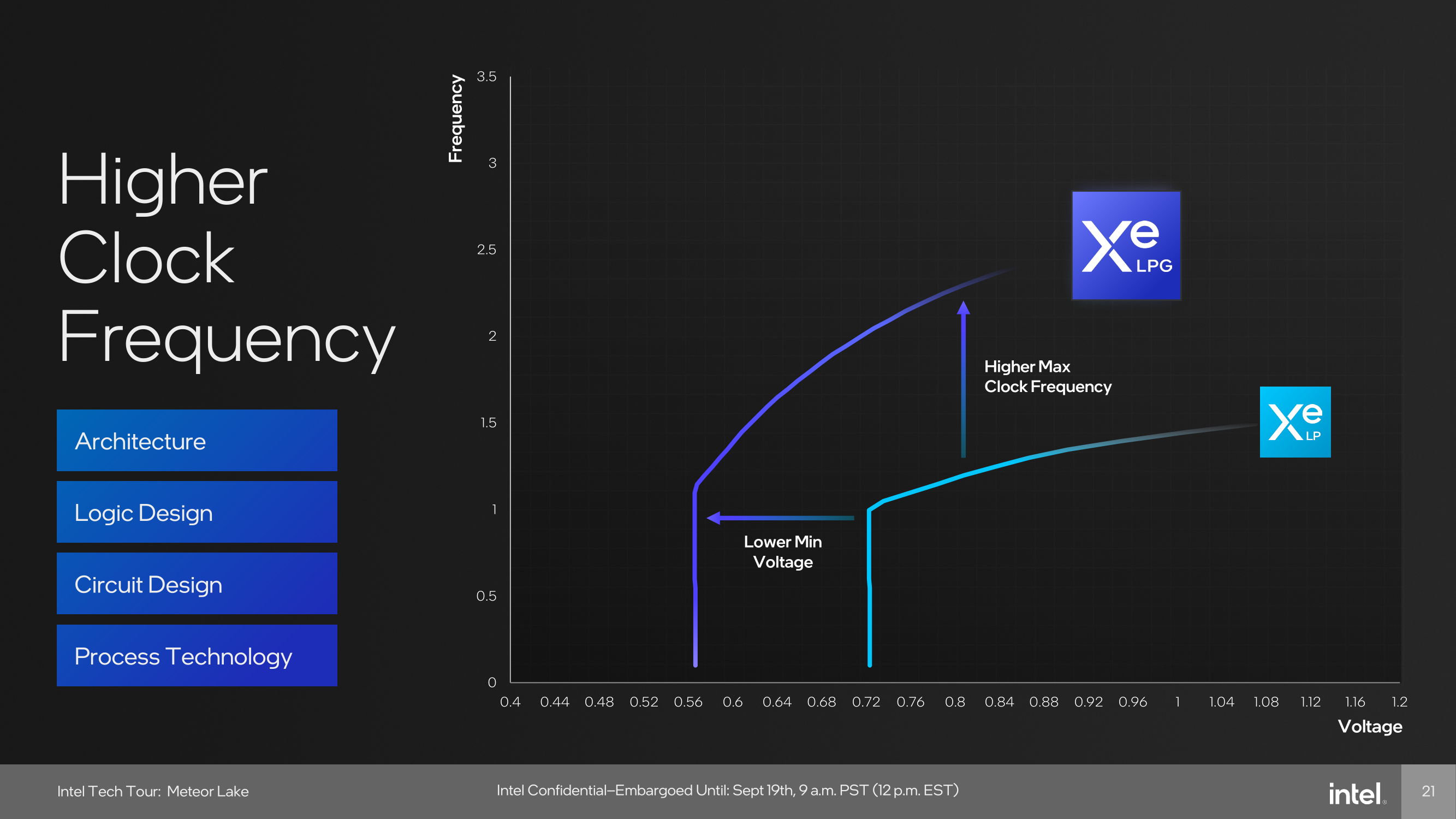
Intel Xe-LPG is the next step up from Xe LP, and one area where performance and efficiency gains are made is through a lower voltage frequency (V/F) curve, allowing the graphics to run at a lower minimum voltage with a higher maximum core clock speed. Intel has also optimized the pipelines for faster frequencies and is claiming up to 2 x performance at iso-voltages, which for a mobile platform such as Meteor Lake, adds more potential with a key focus on achieving a figure of up to 20% in power savings compared to the previous generation.


107 Comments
View All Comments
erinadreno - Tuesday, September 19, 2023 - link
Chiplets on mobile processors doesn't sound exactly enticing. Why does Intel feel the need to use 3 different types of chiplets from 2 foundries on a power-sensitive mobile chip?jazzysoggy - Tuesday, September 19, 2023 - link
It's not the same chiplet strategy as AMD is using for Zen, it's more inline with AMD's MI accelerators. Not as cheap as the Zen strategy, but much more power efficient for power sensitive mobile chips.schujj07 - Tuesday, September 19, 2023 - link
Do you have proof it is more power efficient? Intel right now is vastly less power efficient than AMD and that is regardless of chiplet or monolithic dies.Unashamed_unoriginal_username_x86 - Tuesday, September 19, 2023 - link
First page says .15-.3 pJ/bit for Foveros, AMD has previously stated infinity fabric uses "<2 pJ/bit" which presumably isn't very far under 2. this puts Intel at 5-10x the efficiency for this very specific part of data transmissionduploxxx - Wednesday, September 20, 2023 - link
first generations of infinity fabric were also less power hungry, untill they noticed what is needed to get things faster and there you go. Lots of bandwidth changes and infinity fabric changes and as well the power usage... lets see what Intel is capable of doing first, it's marketing all over the place...Samus - Tuesday, September 19, 2023 - link
Intel is behind AMD on power efficiency purely due to process node. Architecturally they are quite competitive. This is proven in how AMD performance scales when underclocked compared to Intel.Anandtech recently did an investigation into this and came to the conclusion that while the architectures are vastly different they have potentially similar performance once you determine the ideal wattage for the chip, and at the moment Intel is pushing high TDP into extremely inefficient territory to have something competitive with AMD, due to AMD being on a superior node. Basically AMD can deliver X performance at 56w while Intel can deliver X performance at 72w, but Intel can deliver Y performance at 100w while AMD delivers Y performance at 95w.
While impossible to absolutely prove, various factors can help determine this differential has more to do with manufacturing superiority than design superiority.
Intel going for tiles here is a clear attempt to close the gap on this.
PeachNCream - Thursday, September 21, 2023 - link
I think I'd second-guess anything Anandtech does these days. They had one person with an advanced degree that departed years ago after being bought out by Qualcomm when they owned Killer NICs and have since had trouble publishing articles without obvious typos and "in-a-hurry" oversights.On the other hand, if that data is supported by a more credible publisher that has decent measuring equipment and can afford to purchase its own test hardware rather than relying solely on free samples - well then we should sit up and take notice. At this point though, an Anandtech exclusive is just a reason to raise the citation needed flag and THEN further analyze the sources for their motives.
RedGreenBlue - Sunday, October 1, 2023 - link
They’ve always had typos that slip through, or grammar mistakes. All the way back to Anand’s time. I don’t like it but I know what was intended when I see one. There still isn’t another website with the same focus on the segments they focus on. I miss the deep-dives into mobile chips and phones they used to do by investigating what wasn’t publicly released about things but for most people that’s a niche purpose that other sites cover extensively with reviews and can focus on and is a bit too consumer focused and easily found elsewhere. Not really their target market.Composite - Thursday, September 28, 2023 - link
This is indeed similar to MI250 2.5D fabric. However, MI300X is full 3D fabric.elmagio - Tuesday, September 19, 2023 - link
My personal guess, from the moment this was announced, has been that they want every single cm² of silicon going through their Intel 4/EUV capacity going to the compute tile. They're lagging quite a bit behind TSMC and Samsung in terms of EUV capacity, so anything that doesn't stand to benefit much from being designed from the ground up to be made on their own nodes is worth offloading to TSMC.SoC and IO tiles are really not process-limited currently, and their Arc GPUs are in general going manufactured elsewhere anyway. But their CPU design process has always been fully in house every step of the way, and they don't want to change that (at least not yet). So everything but compute would be "wasted" Intel 4 capacity.