The AMD Radeon R9 Fury Review, Feat. Sapphire & ASUS
by Ryan Smith on July 10, 2015 9:00 AM ESTMeet The Sapphire Tri-X R9 Fury OC
Today we’ll be looking at Fury cards from both Sapphire and Asus. We’ll kick things off with Sapphire’s card, the Tri-X R9 Fury OC.
| Radeon R9 Fury Launch Cards | |||||
| ASUS STRIX R9 Fury | Sapphire Tri-X R9 Fury | Sapphire Tri-X R9 Fury OC | |||
| Boost Clock | 1000MHz / 1020MHz (OC) |
1000MHz | 1040MHz | ||
| Memory Clock | 1Gbps HBM | 1Gbps HBM | 1Gbps HBM | ||
| VRAM | 4GB | 4GB | 4GB | ||
| Maximum ASIC Power | 216W | 300W | 300W | ||
| Length | 12" | 12" | 12" | ||
| Width | Double Slot | Double Slot | Double Slot | ||
| Cooler Type | Open Air | Open Air | Open Air | ||
| Launch Date | 07/14/15 | 07/14/15 | 07/14/15 | ||
| Price | $579 | $549 | $569 | ||
Sapphire is producing this card in two variants, a reference clocked version and a factory overclocked version. The version we’ve been sampled is the factory overclocked version, though other than some basic binning to identify cards that can handle being overclocked, the two cards are physically identical.
As far as Sapphire’s overclock goes, it’s a mild overclock, with the card shipping at 1040MHz for the GPU while the memory remains unchanged at 1Gbps. As we discussed in our R9 Fury X review, Fiji cards so far don’t have much in the way of overclocking headroom, so AMD’s partners have to take it easy on the factory overclocks. Sapphire’s overclock puts the upper-bound of any performance increase at 4% – with the real world gains being smaller – so this factory overclock is on the edge of relevance.
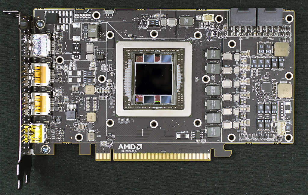
Getting down to the nuts and bolts then, Sapphire’s card is a semi-custom design, meaning Sapphire has paired an AMD reference PCB with a custom cooler. The PCB in question is AMD’s PCB from the R9 Fury X, so there’s little new to report here. The PCB itself measures 7.5” long and features AMD’s 6 phase power design, which is designed to handle well over 300W. For overclockers there is still no voltage control options available for this board design, though as Sapphire has retained AMD’s dual BIOS functionality there’s plenty of opportunity for BIOS modding.
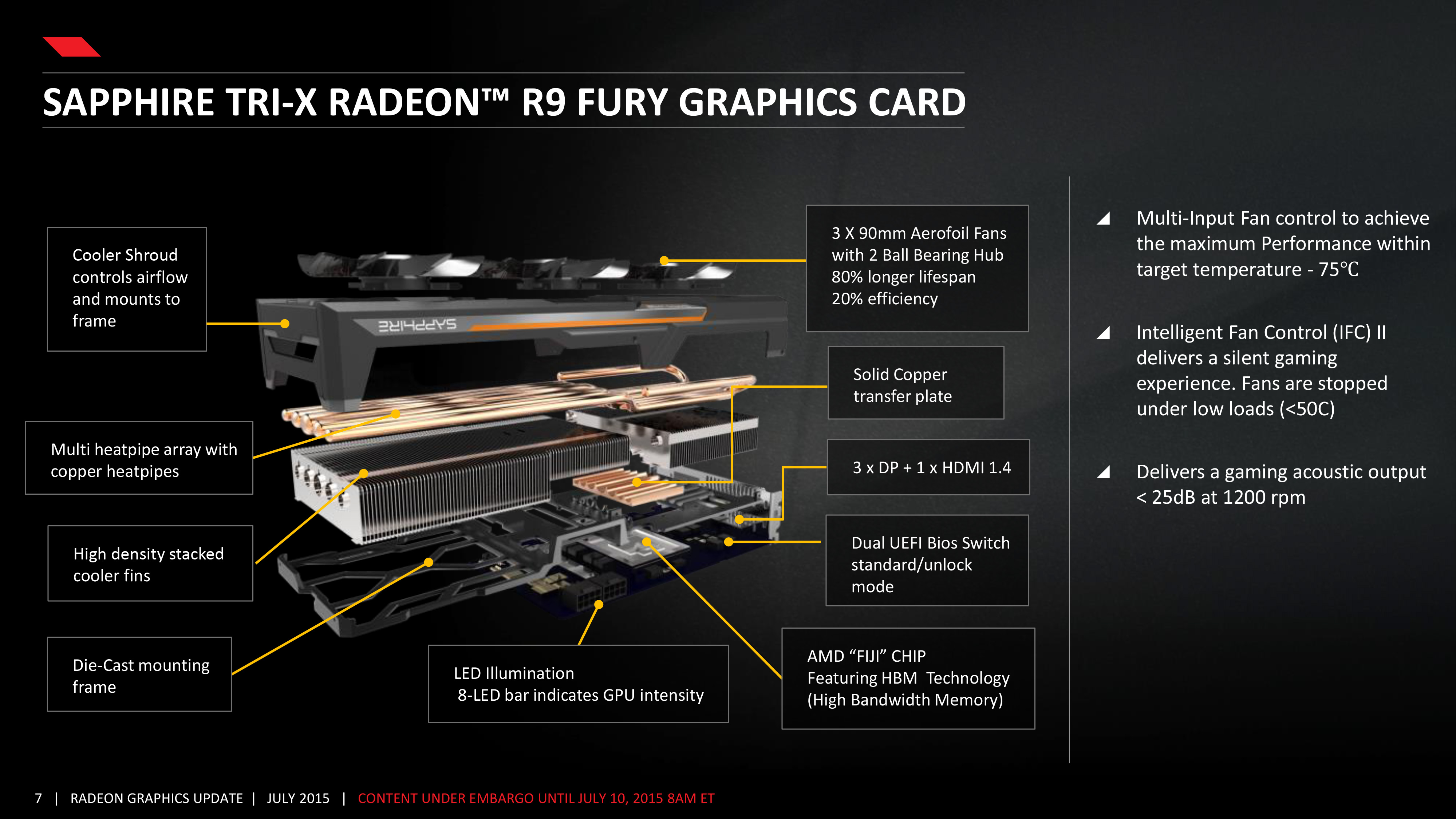
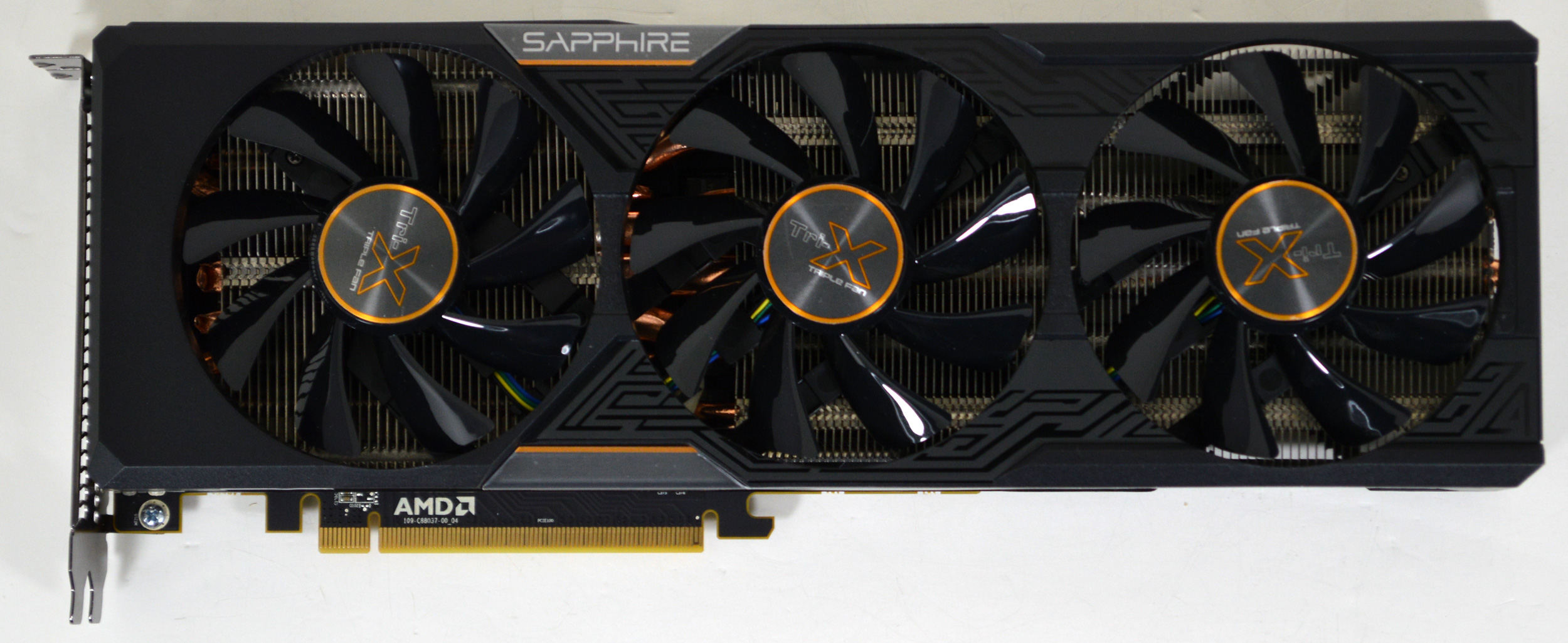
The real story here is Sapphire’s Tri-X cooler, which gets the unenviable job of replacing AMD’s closed loop liquid cooler from the R9 Fury X. With a TBP of 275W Sapphire needs to be able to dissipate quite a bit of heat to keep up with Fiji, which has led to the company using one of their Tri-X coolers. We’ve looked at a few different Tri-X cards over the years, and they have been consistently impressive products. For the Tri-X R9 Fury, Sapphire is aiming for much the same.

Overall the Tri-X cooler used on the Tri-X R9 Fury ends up being quite a large cooler. Measuring a full 12” long it runs the length of the PCB and then some, meanwhile with that much copper and aluminum it’s not a light card either. The end result is that with such a large cooler the card is better defined as a PCB mounted on a cooler than a cooler mounted on a PCB, an amusing juxtaposition from the usual video card. As a result of this Sapphire has gone the extra mile to ensure that the PCB can support the cooler; there are screws in every last mounting hole, there’s a full-sized backplate to further reinforce the card, and the final 4.5” of the cooler that isn’t mounted to the PCB has its own frame to keep that secure as well.
Moving to the top of the card, the Tri-X R9 Fury features three of Sapphire’s 90mm “Aerofoil” fans, the company’s larger, dual ball bearing fans. These fans are capable of moving quite a bit of air even when moving at relatively low speeds, and as a result the overall card noise is kept rather low even under load, as we’ll see in full detail in our benchmark section.
Meanwhile Sapphire has also implemented their version of zero fan speed idle on the Tri-X R9 Fury, dubbed Intelligent Fan Control, which allows the card to turn off its fans entirely when their cooling capacity isn’t needed. With such a large heatsink the Fiji GPU and supporting electronics don’t require active cooling when idling, allowing Sapphire to utilize passive cooling and making the card outright silent at idle. This is a feature a number of manufacturers have picked up on in the last couple of years, and the silent idling this allows is nothing short of amazing. For Sapphire’s implementation on the Tri-X R9 Fury, what we find is that the fans finally get powered up at around 53C, and power down when the temperature falls below 44C.
| Sapphire Tri-X R9 Fury Zero Fan Idle Points | ||||
| GPU Temperature | Fan Speed | |||
| Turn On | 53C | 27% | ||
| Turn Off | 44C | 23% | ||
Helping the cooling effectiveness of the Tri-X quite a bit is the length of the fans and heatsink relative to the length of the PCB. With the 4.5” of overhang, the farthest fan is fully beyond the PCB. That means that all of the air it pushes through the heatsink doesn’t get redirected parallel to the card – as is the case normally for open air cards – but rather the hot air goes straight through the heatsink and past it. For a typical tower case this means that hot air goes straight up towards the case’s exhaust fans, more efficiently directing said hot air outside of the case and preventing it from being recirculated by the card’s fans. While this doesn’t make a night & day difference in cooling performance, it’s a neat improvement that sidesteps the less than ideal airflow situation the ATX form factor results in.
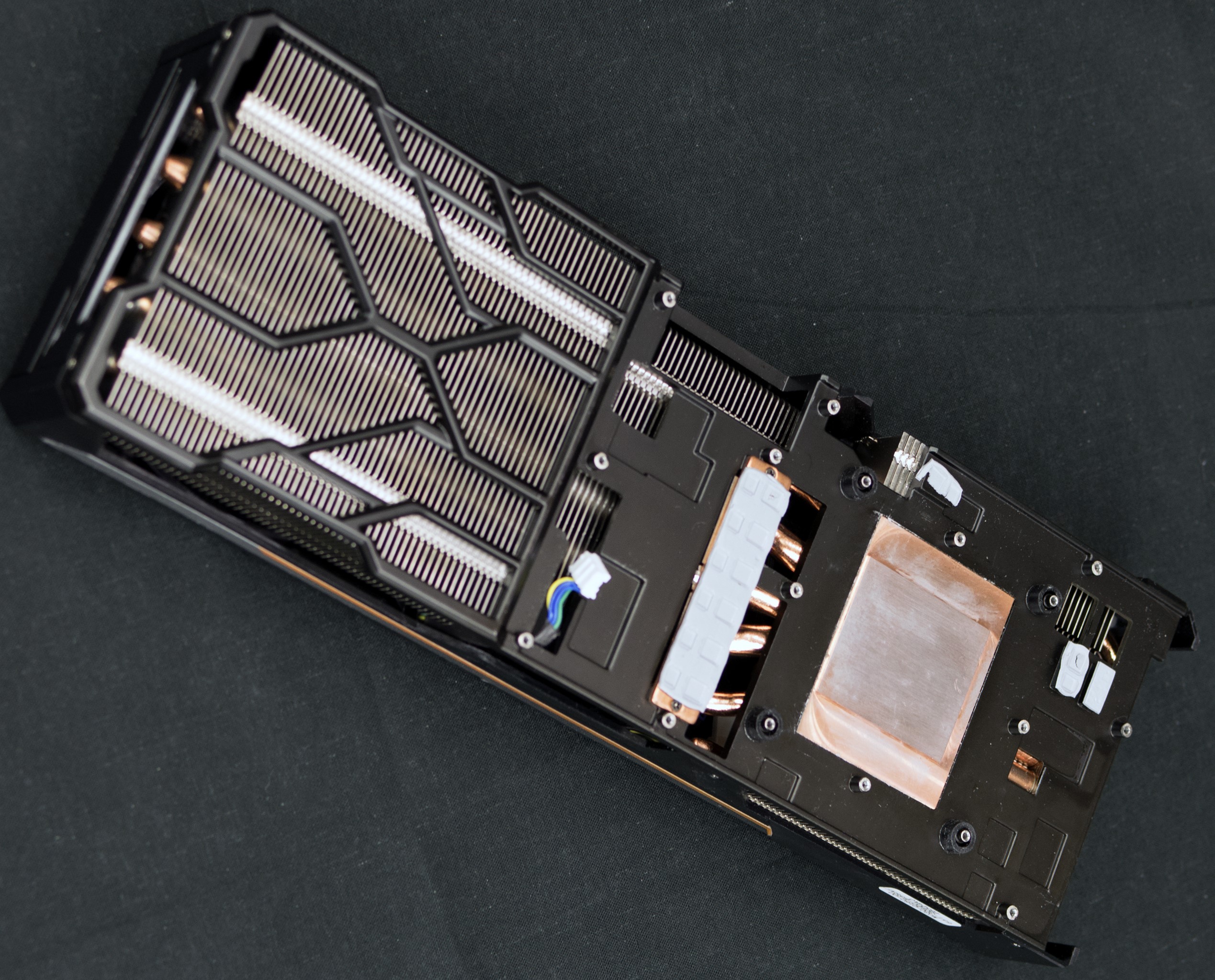
Moving on, let’s take a look at the heatsink itself. The Tri-X’s heatsink runs virtually the entire length of the card, and is subdivided into multiple segments. Connecting these segments are 7 heatpipes, ranging in diameter between 6mm and 10mm. The heatpipes in turn run through both a smaller copper baseplate that covers the VRM MOSFETs, and a larger copper baseplate that covers the Fiji GPU itself. Owners looking to modify the card or otherwise remove the heatsink will want to take note here; we’re told that it’s rather difficult to properly reattach the heatsink to the card due to the need to perfectly line up the heatsink and mate it with the GPU and the HBM stacks.
The Tri-X R9 Fury’s load temperatures tend to top out at 75C, which is the temperature limit Sapphire has programmed the card for. As with the R9 Fury X and the reference Radeon 290 series before that, Sapphire is utilizing AMD’s temperature and fan speed target capabilities, so while the card will slowly ramp up the fan to 75C, once it hits that temperature it will more greatly ramp up the fan to keep the temperature at or below 75C.
Moving on, since Sapphire is using AMD’s PCB, this means the Tri-X also inherits the former’s BIOS and lighting features. The dual-BIOS switch is present, and Sapphire ships the card with two different BIOSes. The default BIOS (switch right) uses the standard 300W ASIC power limit and 75C temperature target. Meanwhile the second BIOS (switch left) Increases the power and temperature limits to 350W and 80C respectively, for greater overclocking limits. Note however that this doesn’t change the voltage curve, so Fury cards in general will still be held back by a lack of headroom at stock voltages. As for the PCB’s LEDs, Sapphire has retained those as well, though they default to blue (sapphire) rather than AMD red.

Finally, since this is the AMD PCB, display I/O remains unchanged. This means the Tri-X offers 3x DisplayPorts along with a single HDMI 1.4 port.

Wrapping things up, the OC version we are reviewing today will retail for $569, $20 over AMD’s MSRP. The reference clocked version on the other hand will retail at AMD’s MSRP of $549, the only launch card that will be retailing at this price. Finally, Sapphire tells us that the OC version will be the rarer of the two due to its smaller run, and that the majority of Tri-X R9 Fury cards that will be on sale will be the reference clocked version.


288 Comments
View All Comments
bill.rookard - Friday, July 10, 2015 - link
Impressive results, especially by the Sapphire card. The thing I'm glad to see is that it's such a -quiet- card overall. That bodes well for some of the next releases (I'm dying to see the results of the Nano) and bodes well for AMD overall.Two things I'd like to see:
1) HBM on APU. Even if it were only 1GB or 2GB with an appropriate interface (imaging keeping the 4096 bit interface and either dual or quad-pumping the bus?). The close location of being on-die and high speed of the DRAM would be a very, VERY interesting graphics solution.
2) One would expect that with the cut down on resources, there would have been more of a loss in performance. On average, you see a 7-8% drop in speed after a loss of 13-14% cut in hardware resources and a slight drop in clock speeds. So - where does that mean the bottleneck in the card is? It's possible that something is a bit lopsided internally (it does however perform exceptionally well), so it would be very interesting to tease out the differences to see whats going on inside the card.
mr_tawan - Friday, July 10, 2015 - link
It would be very interesting to run HBM as the system ram instead of DDR on APU. 4GB (for the 1) wouldn't be a lot and may choke on heavy work load, but for casual user (and tablet uses) that's probably enough.It would also allow smaller machine than NUC form factor, I think.
looncraz - Friday, July 10, 2015 - link
HBM wouldn't be terribly well suited for system RAM due to its comparatively low small-read performance and physical form factor. On an APU, for example, it would probably be best used as a single HBM[2] chip on a 1024-bit bus. Probably just 1 or 2GB, largely dedicated to graphics. That is 128GB/s with HBM1 (but 1GB max), 256GB/s with HBM2 (with, IIRC, 4GB max).For a SoC, though, such as the NUC form factor, as you mentioned, it is potentially a game changer only AMD can deliver on x86. Problem is that the net profit margins in that category are quite small, and AMD needs to be chasing higher net margin markets (net margin being a simple result of market volume, share, and product margin).
I'd love to see it, though, for laptops. And with Apple and AMD being friendly, we may end up seeing it. As well as probably seeing it find its way into the next generation of consoles.
Oxford Guy - Saturday, July 11, 2015 - link
Given the high prices Intel is charging for its NUC systems are you really certain it's not profitable? Perhaps sales aren't good because they're overpriced.Stuka87 - Friday, July 10, 2015 - link
The only way to keep the 4096bit bus would be to use four HBM chips, and I highly doubt this would be the case. I am thinking an APU would use either a single HBM chip, or possibly two. The performance boost would still be huge.ajlueke - Friday, July 10, 2015 - link
1) I can't imagine we won't see this. APU scaling with RAM speed was pretty well documented, I would be surprised if there were socket AM4 motherboards that incorporated some amount of HBM directly. Also, AMD performs best against NVidia at 4K, suggesting that Maxwell may be running into a memory bandwidth bottleneck itself. It will be interesting to see how Pascal performs when you couple a die-shrink with the AMD developed HBM2.2) It does suggest that Fiji derives far more benefit from faster clocks versus more resources. That makes the locked down voltages for the Fury X even more glaring. You supply a card that is massively overpowered, with 500W of heat dissipation but no way to increase voltages to really push the clock speed? I hope we get custom BIOS for that card soon.
silverblue - Saturday, July 11, 2015 - link
As regards APU scaling, it's a tough one. More bandwidth is good, however scaling drops above 2133MHz which shows you'd need more hardware to consume it. Would you put in more shaders, or ROPs? I'd go for the latter - don't APUs usually top out at 8 ROPs? Sure, add in more bandwidth, but at the very least, increase how much the APU can actually draw. The HD 4850 had 32 TMUs (like the 7850K) but 16 ROPs, which is double that on offer here.I keep seeing complaints about AMD's ROP count, so perhaps there's some merit to them.
Nagorak - Sunday, July 12, 2015 - link
It's hard to say what the bottleneck is with memory scaling on APUs. It could be something related to the memory controller built into the CPU rather than the GPU not having the resources to benefit.silverblue - Monday, July 13, 2015 - link
Isn't there a 256-bit Radeon Memory Bus link between memory and the GPU? Just a question.Stuka87 - Friday, July 10, 2015 - link
Is it just me, or is the 290X faster now than it used to be when compared to the 980? Perhaps the 15.7 drivers offered some more performance?