The AMD Radeon R9 Fury X Review: Aiming For the Top
by Ryan Smith on July 2, 2015 11:15 AM ESTHigh Bandwidth Memory: Wide & Slow Makes It Fast
Architecturally, the single most notable addition to AMD’s collection of technologies for Fiji is High Bandwidth Memory (HBM). HBM is a next-generation memory standard that will ultimately come to many (if not all) GPUs as the successor to GDDR5. HBM promises a significant increase in memory bandwidth through the use of an ultra-wide, relatively low-clocked memory bus, with die stacked DRAM used to efficiently place the many DRAM dies needed to drive the wide bus.
As part of their pre-Fury X launch activities, AMD briefed the press on HBM back in May, offering virtually every detail one could want on HBM, how it worked, and the benefits of the technology. So for today’s launch there’s relatively little that’s new to say on the subject, but I wanted to quickly recap what we have seen so far.
After several years of GDDR5 – first used on the Radeon HD 4870 in 2008 – HBM comes at a time where GDDR5 is reaching its limits, and companies have been working on its successors. As awesome as GDDR5 is (and it delivers quite a bit of memory bandwidth compared to just about anything else), GDDR5 is already a bit of a power hog and rather complex to implement. GDDR5’s immediate successors would deliver more bandwidth, but they would also exacerbate this problem by drawing even more power and introducing all of the complexity inherent in differential I/O.
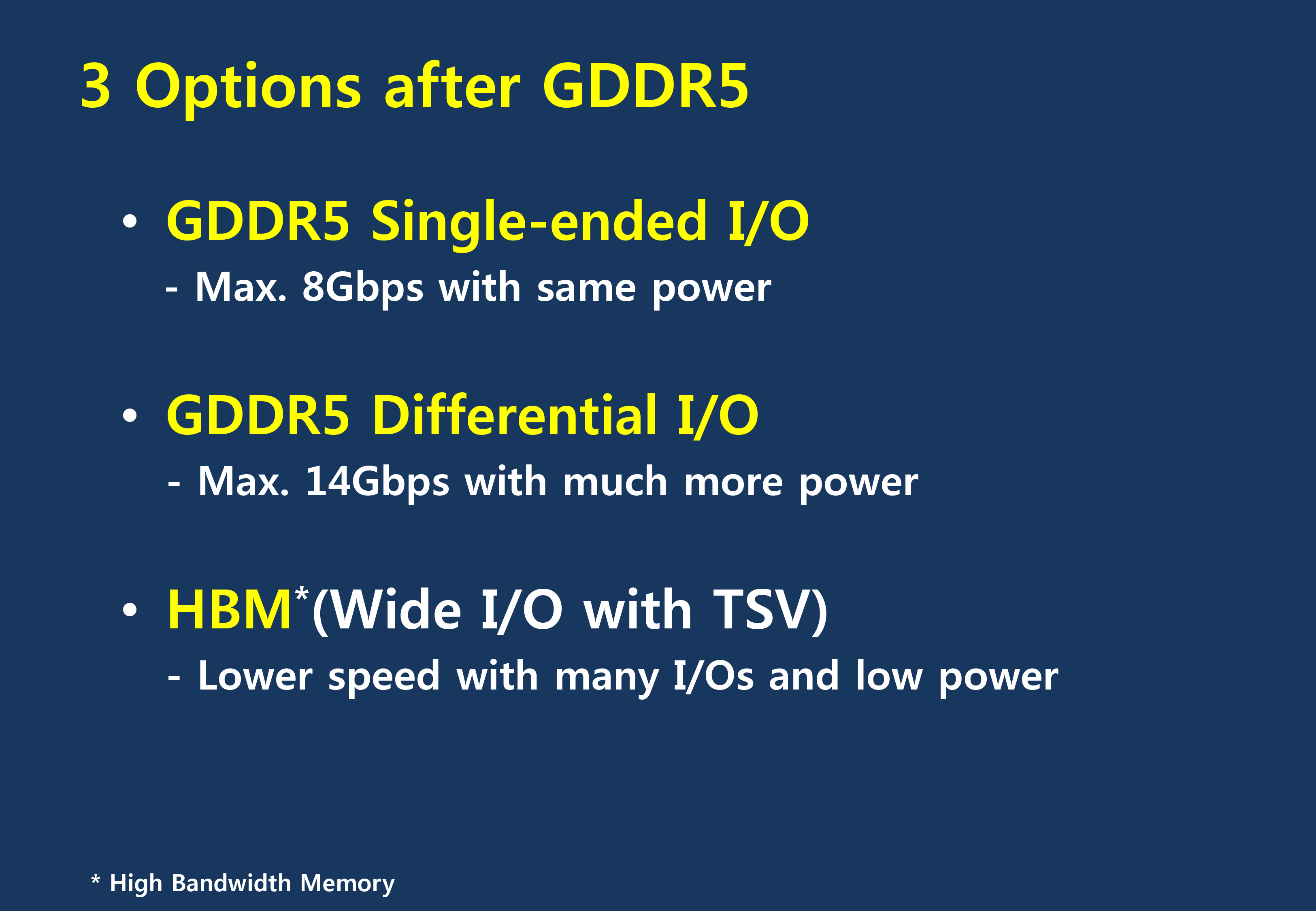
So to succeed GDDR5, AMD, Hynix, and the JEDEC as a whole have taken a very different path. Rather than attempting to push a very high bandwidth, narrow(ish) memory bus standard even higher, they have opted to go in the opposite direction with HBM. HBM would significantly back off of the clockspeeds used, but in return it would go wider than GDDR5. Much, much wider.
The ultimate direction that HBM takes us is with a very wide memory bus clocked at a low frequency. For Fiji, AMD has a 4096-bit memory bus clocked at 1000MHz (500MHz DDR). The use of such a wide bus more than offsets the reduction in clockspeed, allowing R9 Fury X to deliver 60% more memory bandwidth than the R9 290X’s GDDR5 implementation.
On the technical side of things, creating HBM has required a few different technologies to be created/improved in order to assemble the final product. The memory bus itself is rather simple (which is in and of itself a benefit), but a 4096-bit wide memory bus is by conventional standards absurdly wide. It requires thousands of contacts and traces, many times more than even 512-bit GDDR5 required (and that was already a lot).
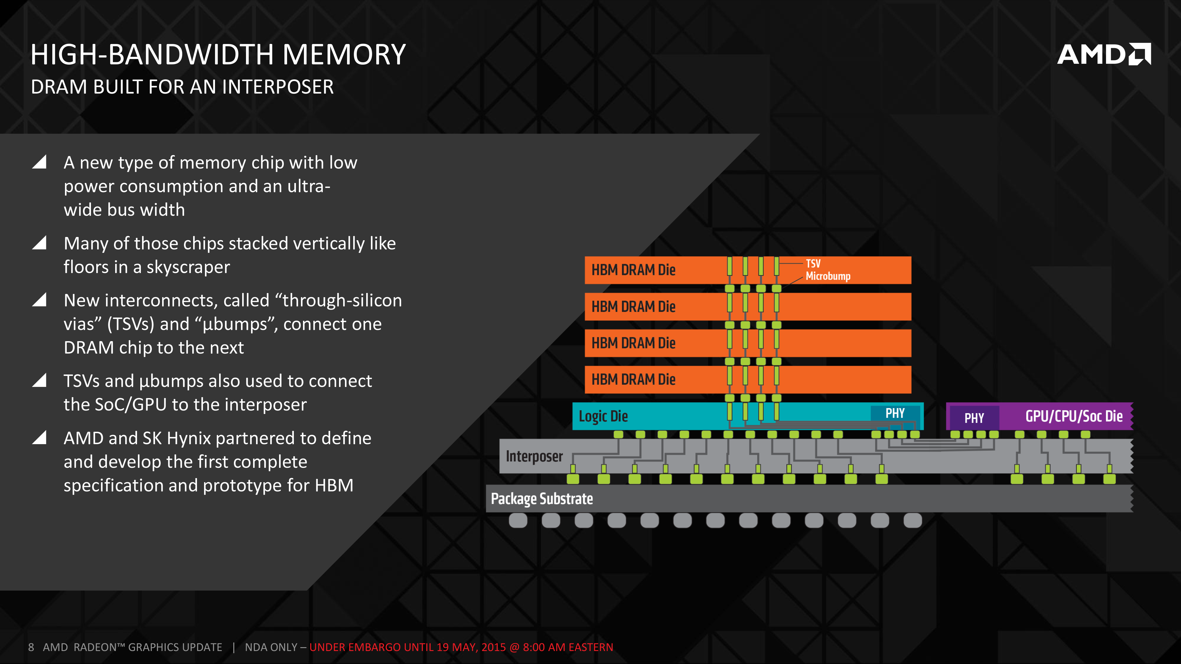
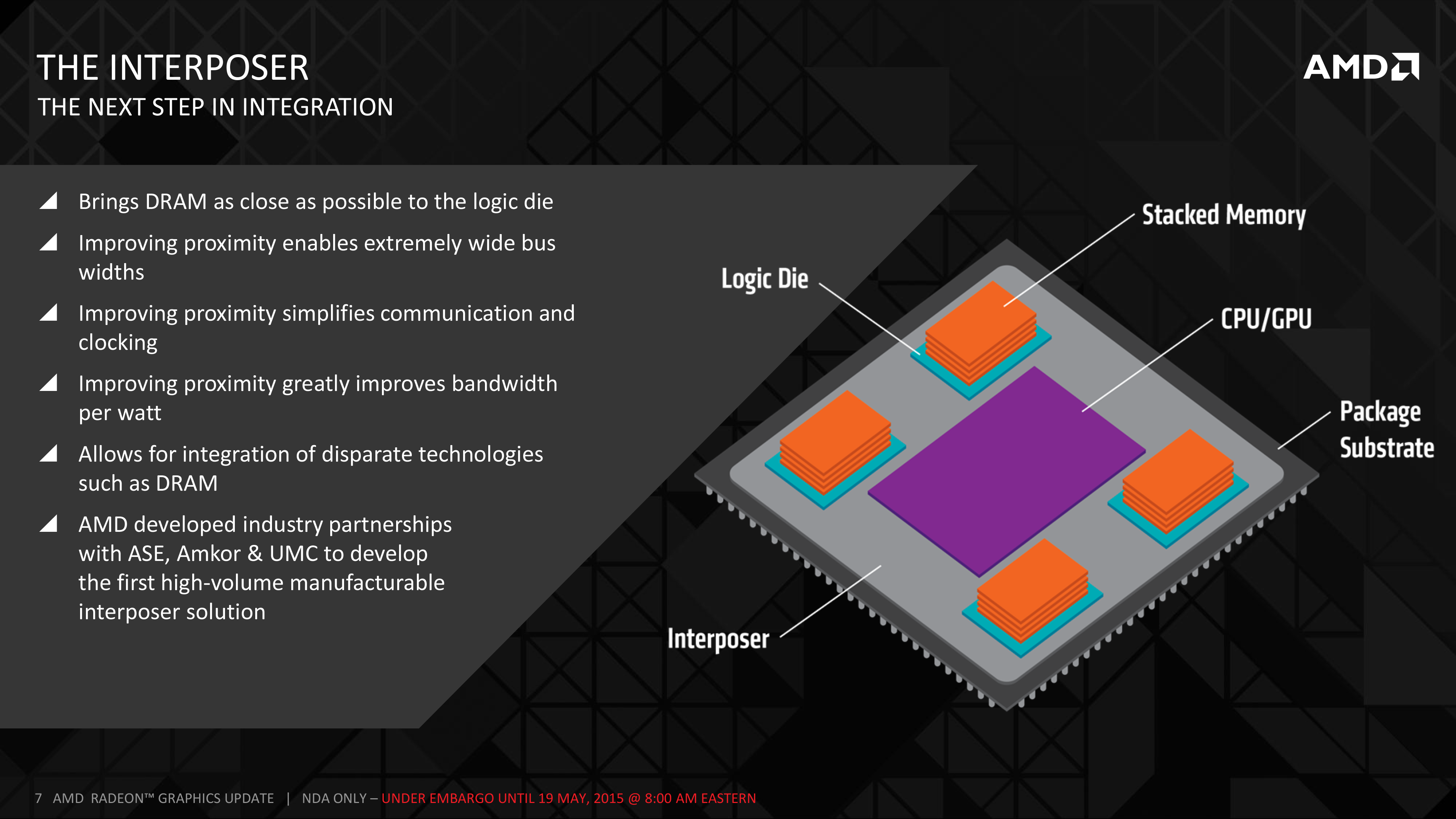
To solve this problem HBM introduces the concept of a silicon interposer. With traditional packaging not up to the challenge of routing so many traces, the one material/package that is capable of hitting the necessary density is fabbed silicon, and thus the silicon interposer. Essentially a partially fabbed chip with just the metal layers but no logic, the interposer is a large chip whose purpose is to allow the ultra-wide 4096-bit memory bus to be created between a GPU and its VRAM, implemented as traces in the metal layers. The interposer itself is not especially complex, however because of the sheer size of the interposer (it needs to be large enough to hold the GPU and VRAM) the interposer brings with it its own challenges.
Meanwhile even though the interposer solves the immediate challenges of implementing a 4096-bit memory bus, the next issue that crops up is where to put the necessary DRAM dies. It takes 16 dies at 256-bits wide each to create the 4096-bit memory bus, and even at its largest size the interposer is still a fraction of the size of the PCB space that traditional GDDR5 chips occupy. As a result the DRAM required for an HBM solution needed to be denser than ever before in a 2D sense.
The solution to that problem was the creation of die-stacking the DRAM. If you can’t go wider, go taller, which is exactly what has happened with HBM. In HBM1 the stacks can go up to 4 dies high, allowing the necessary 16 dies to be reduced to a far more easily managed 4 stacks. With a base logic die at the bottom of each stack to serve as the PHY between the DRAM and the GPU (technically making the complete stack 5 dies), stacking the DRAM is what makes it practical to put so much RAM so close to the GPU.
The final new piece of technology in HBM comes in the die stacks themselves. With the need to route a 1024-bit memory bus through 4 memory dies, traditional package-on-package wire bonding is no longer sufficient. To connect up the memory dies, much like the interposer itself, a newer, denser connectivity method is required.

TSVs. Image Courtesy The International Center for Materials Nanoarchitectonics
To solve that problem, the HBM memory stacks implement Through-Silicon Vias, which involves running the vias straight through silicon devices in order to connect layers. The end result is something vaguely akin to DRAM dies surface mounted on top of each other via microbumps, but with the ability to communicate through the layers. From a manufacturing standpoint, between the silicon interposer and TSVs, TSVs are the more difficult technology to master as it essentially combines all the challenges of DRAM fabbing with the challenges of stacking those DRAM dies on top of each other.
Combined together as a single product, HBM is the next generation of GPU memory technology thanks to the fact that it offers multiple benefits over GDDR5. Memory bandwidth of course is a big part, but of similar significance is the power savings from HBM. The greatly simplified memory bus requires far less power be spent on the bus itself, and as a result the amount of power spent on VRAM is reduced. As we discussed earlier AMD is looking at a 20-30W VRAM power savings on R9 Fury X over R9 290X.
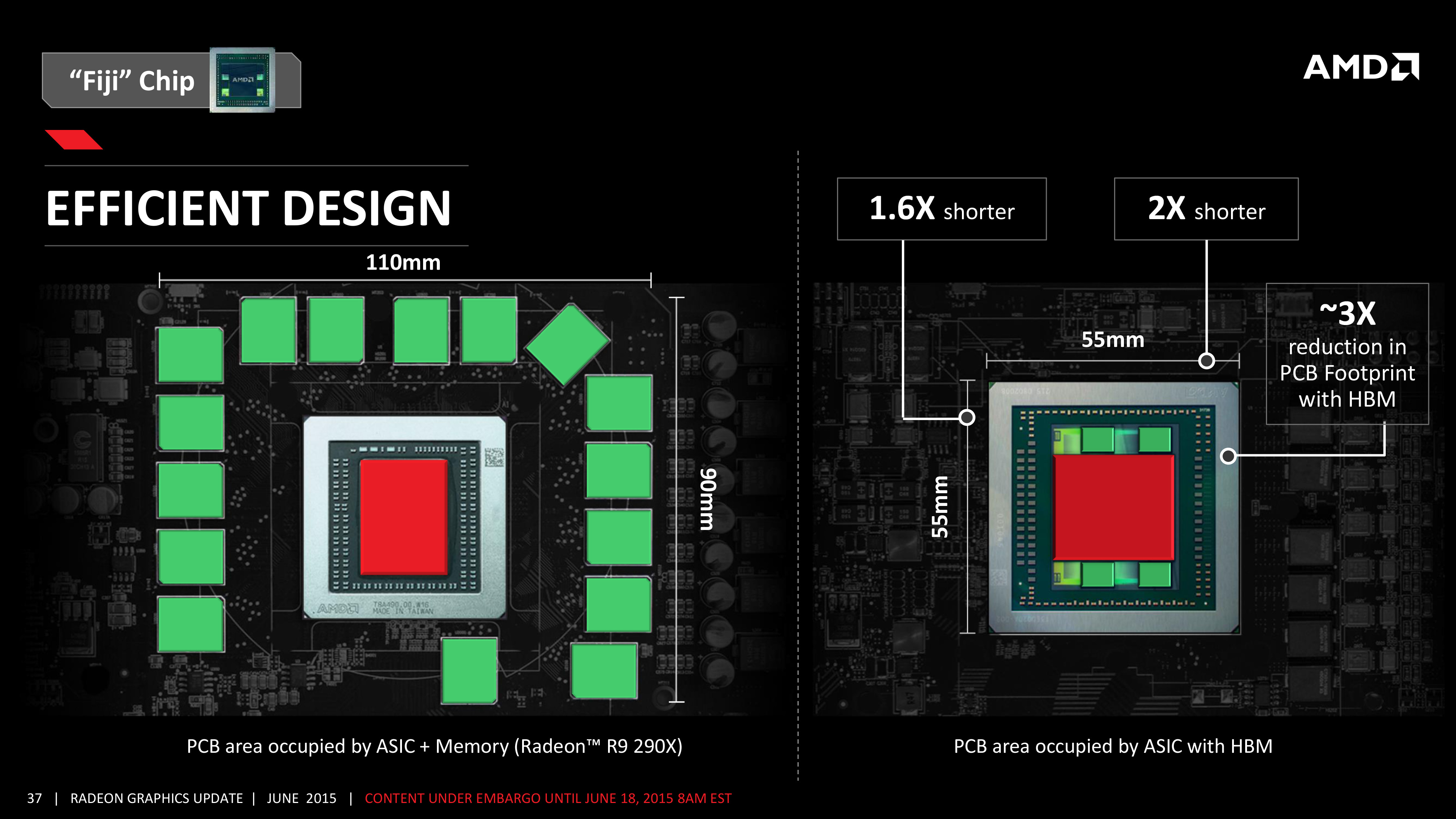
The third major benefit of HBM over GDDR5 goes back to the size benefits discussed earlier. Because all of the VRAM in an HBM setup fits on-chip, this frees up a significant amount of space. The R9 Fury X PCB is 3” shorter than the R9 290X PCB, and the bulk of these savings come from the space savings enjoyed by using HBM. Along with the immediate space savings of 4 small HBM stacks as opposed to 16 GDDR5 memory chips, AMD also gets to cut down on the amount of power delivery circuitry needed to support the VRAM, further saving space and some bill of material costs in the process.
On the downside though, it is the bill of materials that is the biggest question hanging over HBM. Since HBM introduces several new technologies there are any number of things that can go wrong, all of which can drive up the costs. Of particular concern is the yield on the HBM memory stacks, as the TSV technology is especially intricate and said to be difficult to master. The interposer on the other hand is simpler, but it still represents something that has never been done before, and AMD admits upfront that the manufacturing facilities being used to create the interposer are old 65nm lines originally used for full chip production. So while the interposer does not approach the cost of a full logic chip, there is still the matter of the existing manufacturing lines being sub-optimal for high-volume low-cost production. Meanwhile AMD does get to enjoy some cost savings as well – the HBM PHYs are certainly much easier to implement than GDDR5 PHYs on Fiji itself, and the overall package is cheaper since it doesn't have GDDR5 memory running through it – though it's unlikely that these savings outweigh the other costs of implementing HBM at this time.
Ultimately AMD Is not willing to discuss HBM costs or yields at this time. Practically speaking it’s not a consumer matter – what matters to video card buyers is the $650 price tag on the R9 Fury X – and from a trade secrets perspective AMD is loath to share too much about what they have learned since they are the first HBM customer and want to enjoy as much of that advantage as is possible. At this point I feel it’s a safe bet that the 4GB HBM implementation on Fiji is costing AMD more than the 4GB (or even 8GB) GDDR5 implementations on Hawaii cards, but beyond that it’s difficult to say much more on costs.
That said, regardless of what the costs are now, HBM will be the future for AMD, and for the GPU industry as a whole. NVIDIA has already committed to using HBM technology for their high-end Pascal GPU in 2016, so AMD will be joined by other parties next year. Meanwhile AMD has much grander plans for HBM, intending to bring it to other products as costs allow. HBM on lower-priced GPUs is practically a given, meanwhile equipping AMD’s APUs with HBM would solve one of the greatest problems AMD faces today on the iGPU performance front, which is that 128-bit DDR3 bottlenecks the iGPU on their Kaveri APUs. AMD could build a better iGPU, if only they had more bandwidth to feed it with. This is a problem HBM is well positioned to solve.
Finally, at the end of the day what can’t be perfectly captured in words is AMD’s pride in being the first to roll out HBM. AMD was the first (and only) company to support GDDR4, they were the first company to support GDDR5, and now they are the first company to support HBM. The company has put significant resources into helping to develop the technology alongside Hynix, UMC, ASE, Amkor, and the JEDEC, and they see the launch of the technology as a testament to their engineering capabilities.
Furthermore they also see the fact that they are first as being a significant advantage going forward, as it means they have a generational advantage on arch-rival NVIDIA in implementing the technology. Case in point, NVIDIA’s first GDDR5 memory controller was by all accounts an underperformer, and it wasn’t until their second generation GDDR5 controller for Kepler that NVIDIA was able to hit (and even exceed) their aimed for memory clockspeeds. Admittedly this comes down to AMD hoping NVIDIA is going to stumble here, but at the end of the day the company is optimistic that all of their work is going to allow them to get more out of HBM than NVIDIA will be able to.


458 Comments
View All Comments
anandreader106 - Thursday, July 2, 2015 - link
@Wreckage Not quite. Cash reserves play a role in evaluating a company's net worth. When AMD acquired ATI, they spent considerable money to do so and plunged themselves into debt. The resulting valuation of AMD was not simply the combined valuations of AMD and ATI pre-acquisition. Far from it.AMD is the undisputed underdog in 2015, and has been for many years before that. That is why Ryan gave so much praise to AMD in the article. For them to even be competitive at the high end, given their resources and competition, is nothing short of impressive.
If you cannot at least acknowledge that, than your view on this product and the GPU market is completely warped. As consumers we are all better off with a Fury X in the market.
Yojimbo - Thursday, July 2, 2015 - link
Yes, NVIDIA was definitely the underdog at the time of the AMD purchase of ATI. Many people were leaving NVIDIA for dead. NVIDIA had recently lost its ability to make chipsets for Intel processors, and after AMD bought ATI it was presumed (rightly so) that NVIDIA would no longer be able to make chipsets for AMD processors. It was thought that the discrete GPU market might dry up with fusion CPU/GPU chips taking over the market.chizow - Thursday, July 2, 2015 - link
Yep, I remember after the merger happened most AMD/ATI fans were rejoicing as they felt it would spell the end of both Nvidia and Intel, Future is Fusion and all that promise lol. Many like myself were pointing out the fact AMD overpayed for ATI and that they would collapse under the weight of all that debt given ATI's revenue and profits didn't come close to justifying the purchase price.My how things have played out completely differently! It's like the incredible shrinking company. At this point it really is in AMD and their fan's best interest if they are just bought out and broken up for scraps, at least someone with deep pockets might be able to revive some of their core products and turn things around.
Ranger101 - Friday, July 3, 2015 - link
Well done Mr Smith. I would go so far as to say THE best Fury X review on the internet barnone. The most important ingredient is BALANCE. Something that other reviews sorely lack.
In particular the PCPer and HardOCP articles read like they were written by the green
goblin himself and consequently suffer a MASSIVE credibility failure.
Yes Nvidia has a better performing card in the 980TI but it was refreshing to see credit
given to AMD where it was due. Only dolts and fanatical AMD haters (I'm not quite sure
what category chizow falls into, probably both and a third "Nvidia shill") would deny that
we need AMD AND Nvidia for the consumer to win.
Thanks Anandtech.
Michael Bay - Friday, July 3, 2015 - link
Except chizow never stated he wishes to see AMD dead.I guess it`s your butthurt talking.
chizow - Friday, July 3, 2015 - link
Yep, just AMD fanboys ;)"What's Left of AMD" can keep making SoCs and console APUs or whatever other widgets under the umbrella of some monster conglomerate like Samsung, Qualcomm or Microsoft and I'm perfectly OK with that. Maybe I'll even buy an AMD product again.
medi03 - Sunday, July 5, 2015 - link
"AMD going away won't matter to anyone but their few remaining devout fanboys'So kind (paid?) nVidia troll chizow is.
chizow - Monday, July 6, 2015 - link
@medi03 no worries I look forward to the day (unpaid?) AMD fantroll's like you can free yourselves from the mediocrity that is AMD.chizow - Friday, July 3, 2015 - link
Yet, still 3rd rate. The overwhelming majority of the market has gone on just fine without AMD being relevant in the CPU market, and recently, the same has happened in the GPU market. AMD going away won't matter to anyone but their few remaining devout fanboys like Ranger101.piiman - Friday, July 3, 2015 - link
"AMD going away won't matter to anyone but their few remaining devout fanboys'Hmmm you'll think different when GPU prices go up up up. Competition is good for consumers and without it you will pay more, literally.