The AMD Radeon R9 Fury X Review: Aiming For the Top
by Ryan Smith on July 2, 2015 11:15 AM ESTDisplay Matters: Virtual Super Resolution, Frame Rate Targeting, and HEVC Decoding
Wrapping up our look at the technical underpinnings of the Fiji GPU, we’ll end things with a look at the display and I/O stack for AMD’s latest GPU.
As a GCN 1.2 part, Fiji inherits most of its capabilities in-place from Tonga. There is one notable exception to this, HEVC, which we’ll get to in a bit, otherwise from a features standpoint you’re looking at the same display feature set as was on Tonga.

For Display I/O this means 6 display controllers capable of driving DVI, HDMI 1.4a, and DisplayPort 1.2a. Unfortunately because Tonga lacked support for HDMI 2.0, the same is true for Fiji, and as a result you can only drive 4k@60Hz displays either via DisplayPort, or via tandem HDMI connections. The good news here is that it will be possible to do active conversion from DisplayPort to HDMI 2.0 later this year, so Fiji is not permanently cut-off from HDMI 2.0, however those adapters aren’t here quite yet and there are still some unresolved questions to be addressed (e.g. HDCP 2.2).
On the multimedia front, Fiji brings with it an enhanced set of features from Tonga. While the video encode side (VCE) has not changed – AMD still supports a wide range of H.264 encode settings – the video decode side has seen a significant upgrade. Fiji is the first AMD discrete GPU to support full hardware HEVC decoding, coinciding with the launch of that feature on the GCN 1.2-based Carrizo APU as well.
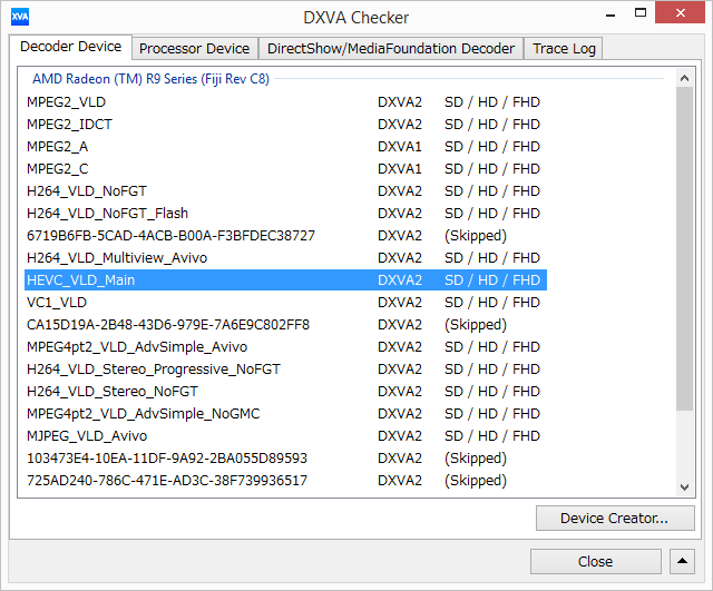
A look at DXVA Checker confirms the presence of Main Profile (HEVC_VLD_Main) support, the official designation for 8-bit color support. Main profile is expected to be the most common profile level for HEVC content, so Fiji’s support of just Main profile should cover many use cases.
Unfortunately what you won’t find here is Main10 profile support, which is the profile for 10-bit color, and AMD has confirmed that 10-bit color support is not available on Fiji. As our in-house video guru Ganesh T S pointed out when looking at these results, Main10 is already being used in places you wouldn’t normally expect to see it, such as Netflix streaming. So there is some question over how useful Fiji’s HEVC decoder will be with commercial content, ignoring for now the fact that lack of Main10 support essentially rules out good support for some advanced color space features such as Rec. 2020, which needs higher bit depths to support the larger color space without extensive banding.
Meanwhile the state of AMD’s drivers with respect to video playback is hit and miss. DXVA Checker crashed when attempting to enumerate 4K resolution support on Fiji, and 4K has been something of a thorn in AMD’s side. This is also likely why Media Player Classic Home Cinema and its built-in LAV Filters are currently ignoring 4K support on Fiji and are falling back to software decoding. As a result 1080p hardware decoding works great on Fiji – both H.264 and HEVC – but getting Fiji to decode 4K content is a lot harder. Using Windows’ built-in H.264 decoder works for 4K H.264 decoding, and in the meantime it’s a bit harder to test Fiji’s HEVC capabilities at 4K since Windows 8 lacks an HEVC decoder.
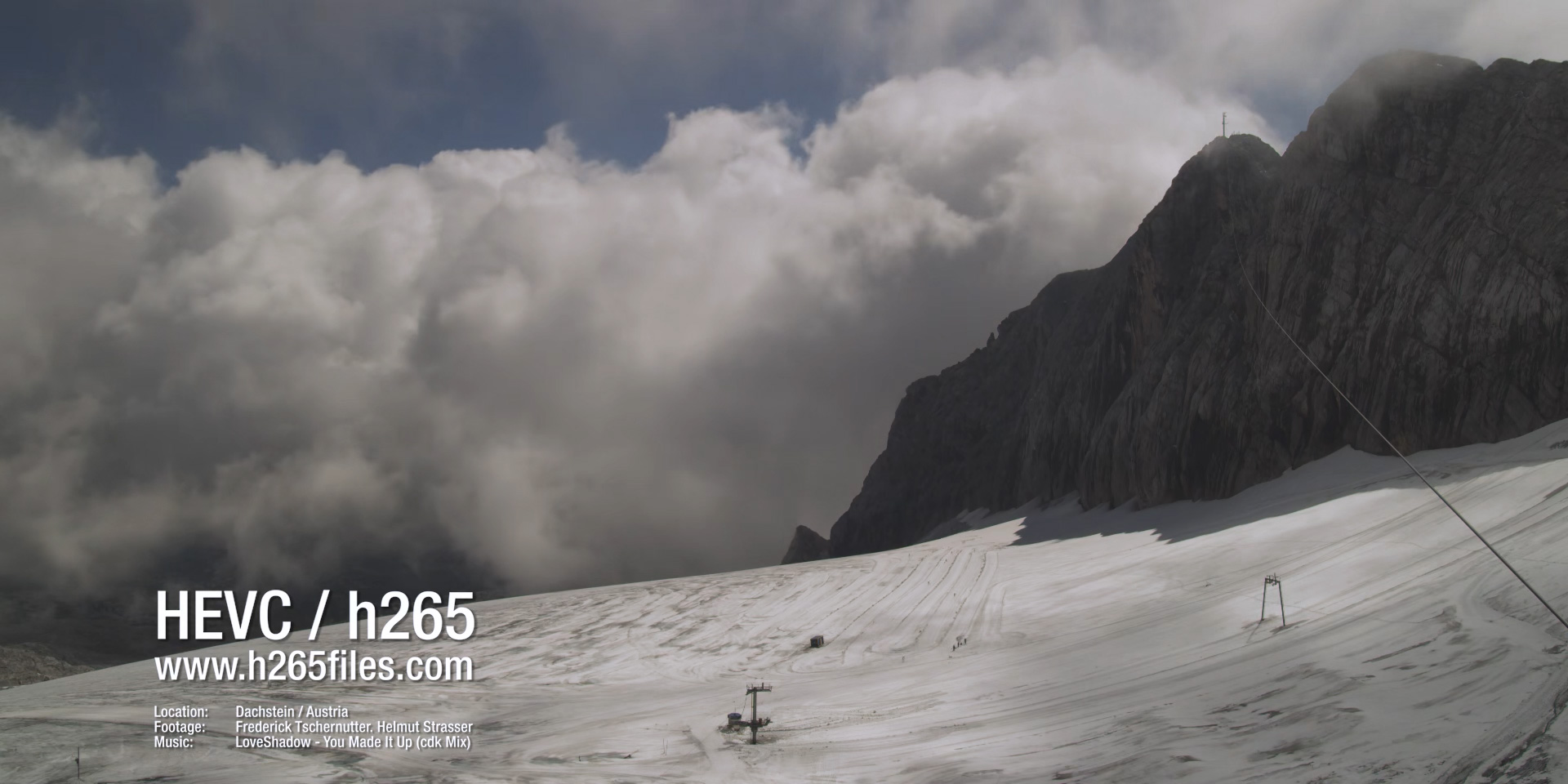
Decoding 1080p HEVC In MPC-HC on Fiji
With full hardware decode support for HEVC still being relatively new in the PC space, I expect we’ll see some teething issues for some time yet. For the moment AMD needs to resolve any crashing issues and get off of LAV’s blacklist, since the LAV filters are by our estimation the most commonly used for generic HEVC media playback.
On a side note, given the fact that the Tonga GPU (R9 285) is the only GCN 1.2 GPU without HEVC decoding, I also took the liberty of quickly loading up a modified copy of the Catalyst 15.15 launch drivers for the R9 300/Fury series, and seeing if HEVC support may have been hidden in there the entire time. Even with these latest drivers, R9 285 does not support HEVC, and while I admittedly wasn’t expecting it to, I suspect there’s more to Tonga’s UVD block given its nature as the odd man out.
Last but not least, TrueAudio support is also included with Fiji. First introduced on AMD’s GCN 1.1 family, TrueAudio is AMD’s implementation of advanced hardware audio processing, powered by a cluster of Tensilica’s HiFi EP DSPs. Despite these DSPs being similar to what’s found on the PS4, we have not seen much in the way of support for TrueAudio in the last year outside of a few AMD-sponsored demos/titles, so thus far it remains an underutilized hardware feature.
Moving on, let’s talk software features. Back in December with their Omega Drivers, AMD introduced Virtual Super Resolution. VSR is AMD’s implementation of downsampling and is essentially the company’s answer to NVIDIA’s DSR technology.
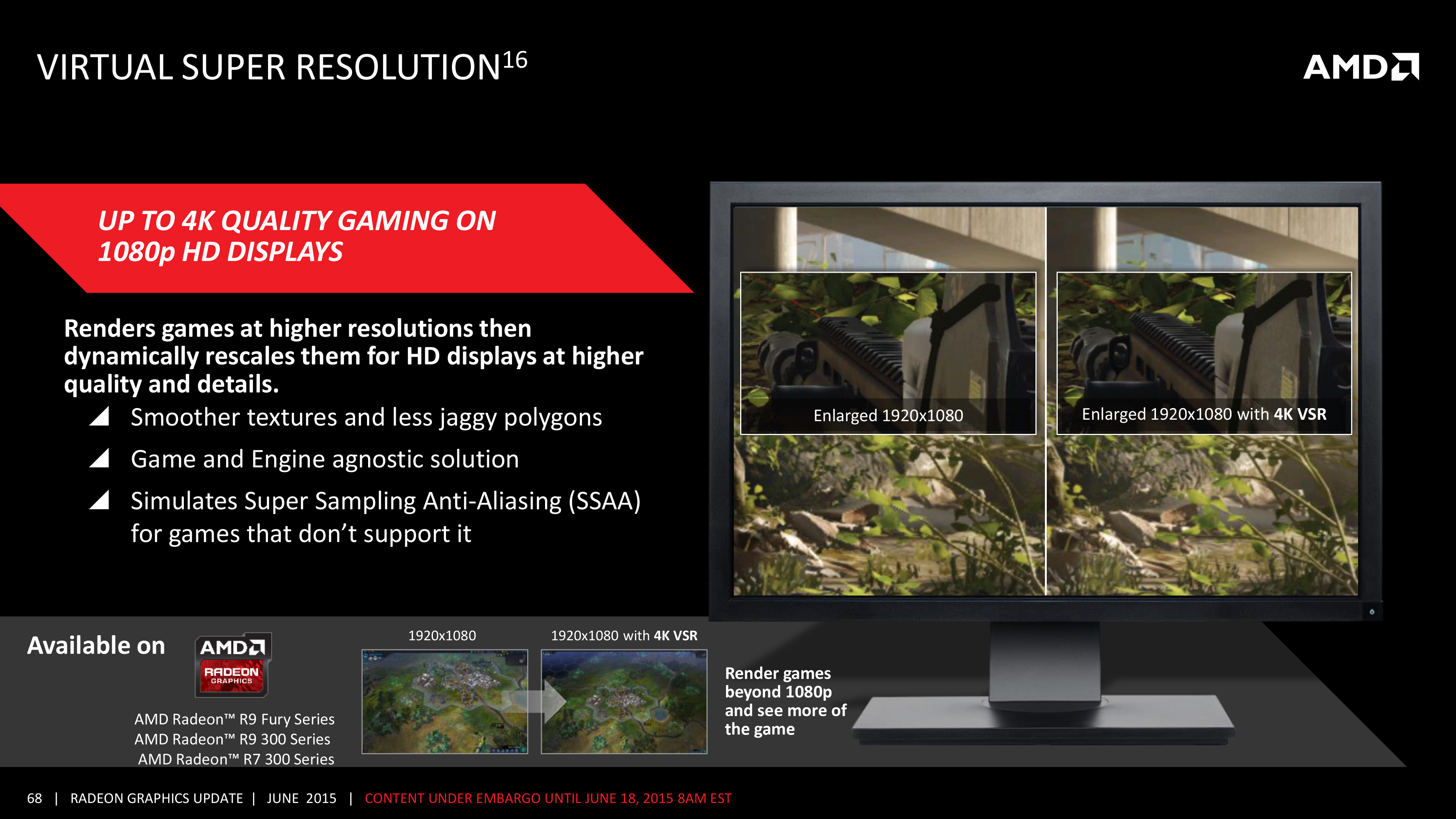
However while VSR and DSR are designed to solve the same problem, the two technologies go about solving it in very different ways. With DSR NVIDIA implemented it as a shader program; it gave NVIDIA a lot of resolution flexibility in exchange for a slight performance hit, and for better or worse they threw in a Gaussian blur by default as well. AMD however opted to implement VSR directly against their display controllers, skipping the shading pipeline and the performance hit at a cost of flexibility.
Due to the nature of VSR and the fact that it heavily relies on the capabilities of AMD’s display controllers, only AMD’s newest generation display controllers offer the full range of virtual resolutions. The GCN 1.1 display controller, for example, could not offer 4K virtual resolutions, so the R9 290X and other high-end Hawaii cards topped out at a virtual resolution of 3200x1800 for 1080p and 1440p displays. With GCN 1.2 however, AMD’s newer display controller supports downsampling from 4K in at least some limited scenarios, and while this wasn’t especially useful for the R9 285, this is very useful for the R9 Fury X.
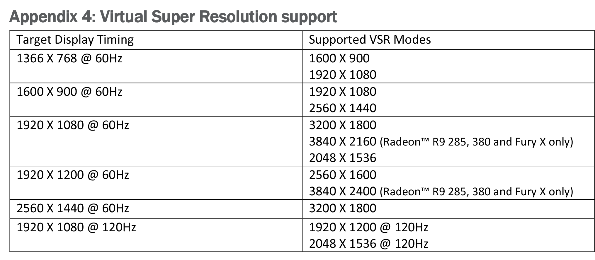
Overall for the R9 Fury X, the notable downsampling modes supported for the card are 3200x1800 (2.77x) and 3840x2160 (4.0x) for a native resolution of 1080p, 2560x1600 (1.77x) and 3840x2400 (4.0x) for a native resolution of 1200p, and unfortunately just 3200x1800 (1.56x) for a native resolution of 1440p. As a result VSR still can’t match the flexibility of DSR when it comes to resolutions, but AMD can finally offer 4K downsampling for 1080p panels, which allows for a nice (but expensive) 2x2 oversampling pattern, very similar to 4x ordered grid SSAA.
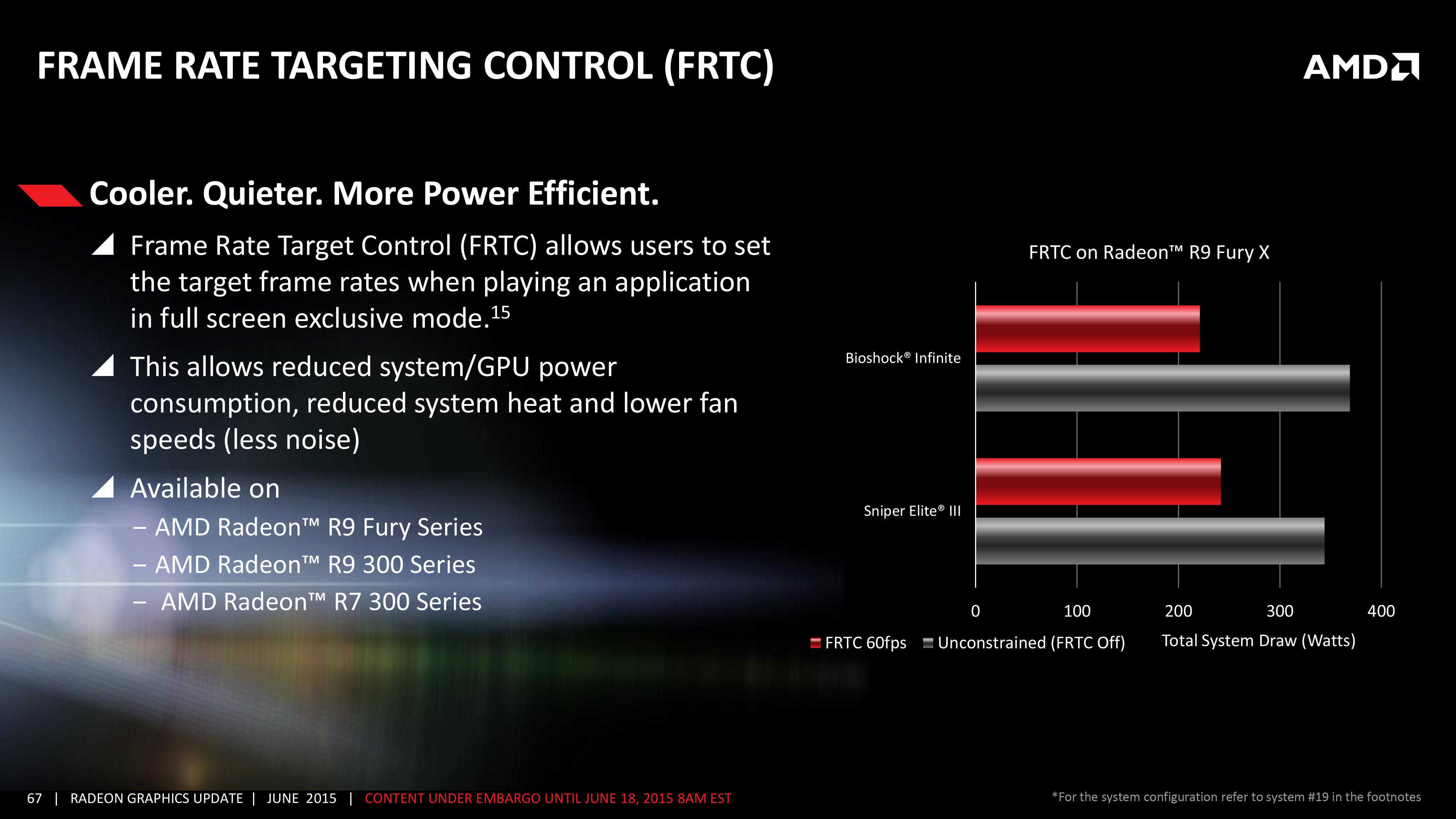
Finally, with AMD’s latest drivers they are also introducing a new framerate capping feature they are calling Frame Rate Target Control (FRTC). FRTC itself is not a new concept – 3rd party utilities such as MSI Afterburner and Radeon Pro have supported such functionality for a number of years now – however the change here is that AMD is finally bringing the technology into their drivers rather than requiring users to seek out 3rd party tools to do the job.
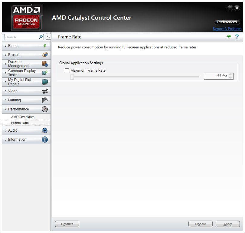
Frame Rate Target Control: From 55 fps to 95 fps
The purpose of FRTC is to allow users to cap the maximum framerate of a game without having to enable v-sync and the additional latency that can come from it, making for an effective solution that not v-sync and yet still places a hard cap on framerates. Note however that this is not a dynamic technology (ala NVIDIA’s Adaptive Sync), so there is no ability to dynamically turn v-sync on and off here. As for why users might want to cap their framerates, this is primarily due to the fact that video cards like the R9 Fury X can run circles around most older games, rendering framerates in to the hundreds at a time when even the fastest displays top out at 144Hz. Capping the frame rate serves to cut down on unnecessary work as a result, keeping the GPU from rendering frames that will never be seen.
AMD is only advertising FRTC support for the 300/Fury series at this time, so there is some question over whether we will see it brought over to AMD’s older cards. Given that AMD’s drivers are essentially split at the moment, I suspect we won’t have our final answer until the drivers get re-unified in a later release (most likely this month).


458 Comments
View All Comments
looncraz - Friday, July 3, 2015 - link
75MHz on a factory low-volting GPU is actually to be expected. If the voltage scaled automatically, like nVidia's, there is no telling where it would go. Hopefully someone cracks the voltage lock and gets to cranking of the hertz.chizow - Friday, July 3, 2015 - link
North of 400W is probably where we'll go, but I look forward to AMD exposing these voltage controls, it makes you wonder why they didn't release them from the outset given they made the claims the card was an "Overclocker's Dream" despite the fact it is anything but this.Refuge - Friday, July 3, 2015 - link
It isn't unlocked yet, so nobody has overclocked it yet.chizow - Monday, July 6, 2015 - link
But but...AMD claimed it was an Overclocker's Dream??? Just another good example of what AMD says and reality being incongruent.Thatguy97 - Thursday, July 2, 2015 - link
would you say amd is now the "geforce fx 5800"sabrewings - Thursday, July 2, 2015 - link
That wasn't so much due to ATI's excellence. It had a lot to do with NVIDIA dropping the ball horribly, off a cliff, into a black hole.They learned their lessons and turned it around. I don't think either company "lost" necessarily, but I will say NVIDIA won. They do more with less. More performance with less power, less transistors, less SPs, and less bandwidth. Both cards perform admirably, but we all know the Fury X would've been more expensive had the 980 Ti not launched where it did. So, to perform arguably on par, AMD is living with smaller margins on probably smaller volume while Nvidia has plenty of volume with the 980 Ti and their base cost is less as they're essentially using Titan X throw away chips.
looncraz - Thursday, July 2, 2015 - link
They still had to pay for those "Titan X throw away chips" and they cost more per chip to produce than AMD's Fiji GPU. Also, nVidia apparently had to not cut down the GPU as much as they were planning as a response to AMD's suspected performance. Consumers win, of course, but it isn't like nVidia did something magical, they simply bit the bullet and undercut their own offerings by barely cutting down the Titan X to make the 980Ti.That said, it is very telling that the AMD GCN architecture is less balanced in relation to modern games than the nVidia architecture, however the GCN architecture has far more features that are going unused. That is one long-standing habit ATi and, now, AMD engineers have had: plan for the future in their current chips. It's actually a bad habit as it uses silicon and transistors just sitting around sucking up power and wasting space for, usually, years before the features finally become useful... and then, by that time, the performance level delivered by those dormant bits is intentionally outdone by the competition to make AMD look inferior.
AMD had tessellation years before nVidia, but it went unused until DX11, by which time nVidia knew AMD's capabilities and intentionally designed a way to stay ahead in tessellation. AMD's own technology being used against it only because it released it so early. HBM, I fear, will be another example of this. AMD helped to develop HBM and interposer technologies and used them first, but I bet nVidia will benefit most from them.
AMD's only possible upcoming saving grace could be that they might be on Samsung's 14nm LPP FinFet tech at GloFo and nVidia will be on TSMC's 16nm FinFet tech. If AMD plays it right they can keep this advantage for a couple generations and maximize the benefits that could bring.
vladx - Thursday, July 2, 2015 - link
Afaik, even though TSMC's GinFet will be 16nm it's a superior process overall to GloFo's 14nm FF so I dount AMD will gain any advantage.testbug00 - Sunday, July 5, 2015 - link
TSMC's FinFET 16nm process might be better than GloFo's own canceled 14XM or whatever they called it.Better than Samsung's 14nm? Dubious. Very unlikely.
chizow - Sunday, July 5, 2015 - link
Why is it dubious? What's the biggest chip Samsung has fabbed? If they start producing chips bigger than the 100mm^2 chips for Apple, then we can talk but as much flak as TSMC gets flak over delays/problems, they still produce what are arguably the world's most advanced seminconductors, right there next to Intel's biggest chips in size and complexity.