The AMD Radeon R9 Fury X Review: Aiming For the Top
by Ryan Smith on July 2, 2015 11:15 AM ESTFiji’s Layout
So what did AMD put in 8.9 billion transistors filling out 596mm2? The answer as it turns out is quite a bit of hardware, though at the same time perhaps not as much (or at least not in the ratios) as everyone was initially hoping for.
The overall logical layout of Fiji is rather close to Hawaii after accounting for the differences in the number of resource blocks and the change in memory. Or perhaps Tonga (R9 285) is the more apt comparison, since that’s AMD’s other GCN 1.2 GPU.
In either case the end result is quite a bit of shading power for Fiji. AMD has bumped up the CU count from 44 to 64, or to put this in terms of the number of ALUs/stream processors, it’s up from 2816 to a nice, round 4096 (2^12). As we discussed earlier FP64 performance has been significantly curtailed in the name of space efficiency, otherwise at Fury X’s stock clockspeed of 1050MHz, you’re looking at enough ALUs to push 8.6 TFLOPs of FP32 operations.
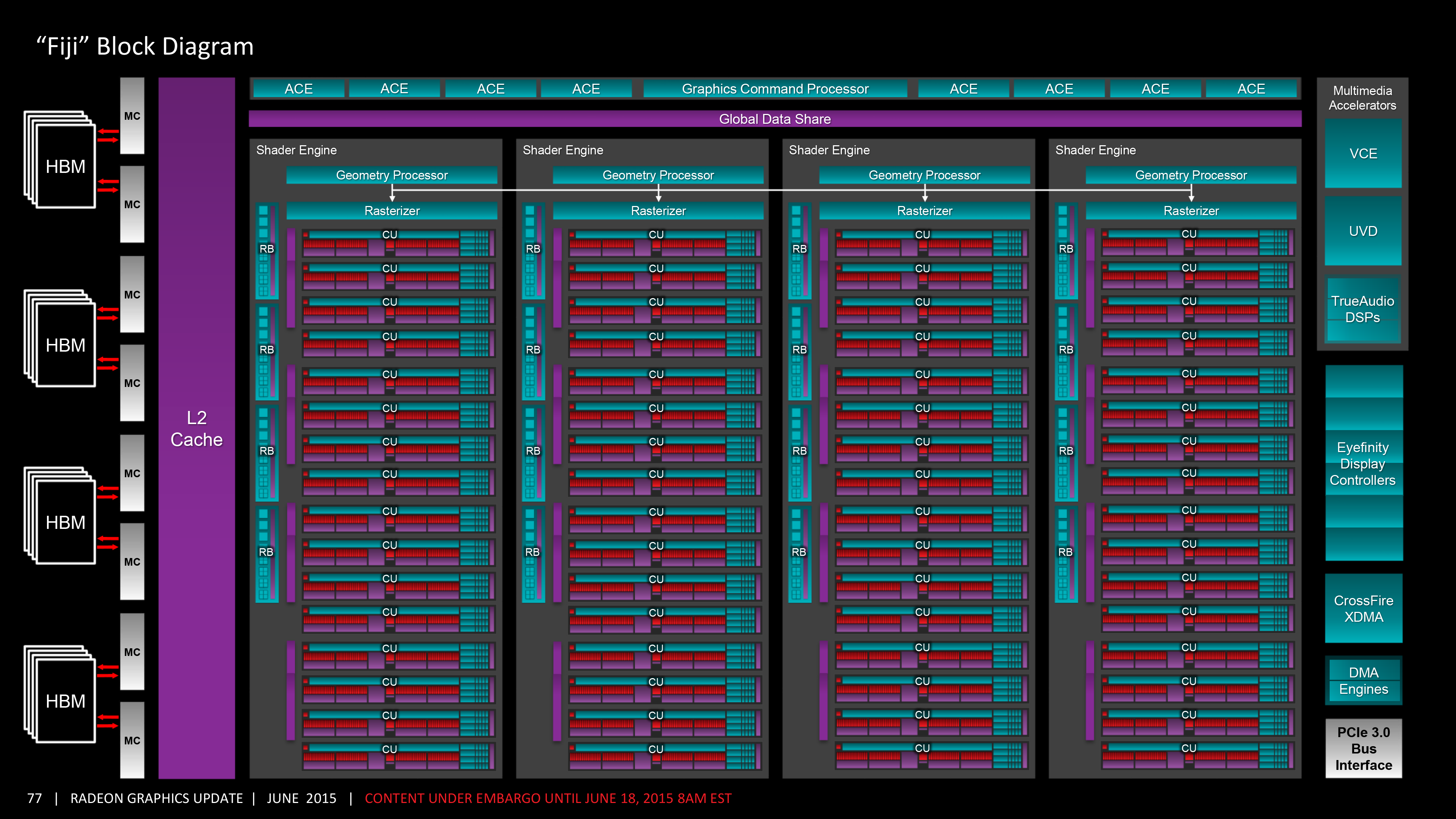
These 64 CUs in turn are laid out in a manner consistent with past GCN designs, with AMD retaining their overall Shader Engine organization. Sub-dividing the GPU into four parts, each shader engine possesses 1 geometry unit, 1 rasterizer unit, 4 render backends (for a total of 16 ROPs), and finally, one-quarter of the CUs, or 16 CUs per shader engine. The CUs in turn continue to be organized in groups of 4, with each group sharing a 16KB L1 scalar cache and 32KB L1 instruction cache. Meanwhile since Fiji’s CU count is once again a multiple of 16, this also does away with Hawaii’s oddball group of 3 CUs at the tail-end of each shader engine.
Looking at the broader picture, what AMD has done relative to Hawaii is to increase the number of CUs per shader engine, but not changing the number of shader engines themselves or the number of other resources available for each shader engine. At the time of the Hawaii launch AMD told us that the GCN 1.1 architecture had a maximum scalability of 4 shader engines, and Fiji’s implementation is consistent with that. While I don’t expect AMD will never go beyond 4 shader engines – there are always changes that can be made to increase scalability – given what we know of GCN 1.1’s limitations, it looks like AMD has not attempted to increase their limits with GCN 1.2. What this means is that Fiji is likely the largest possible implementation of GCN 1.2, with as many resources as the architecture can scale out to without more radical changes under the hood to support more scalability.
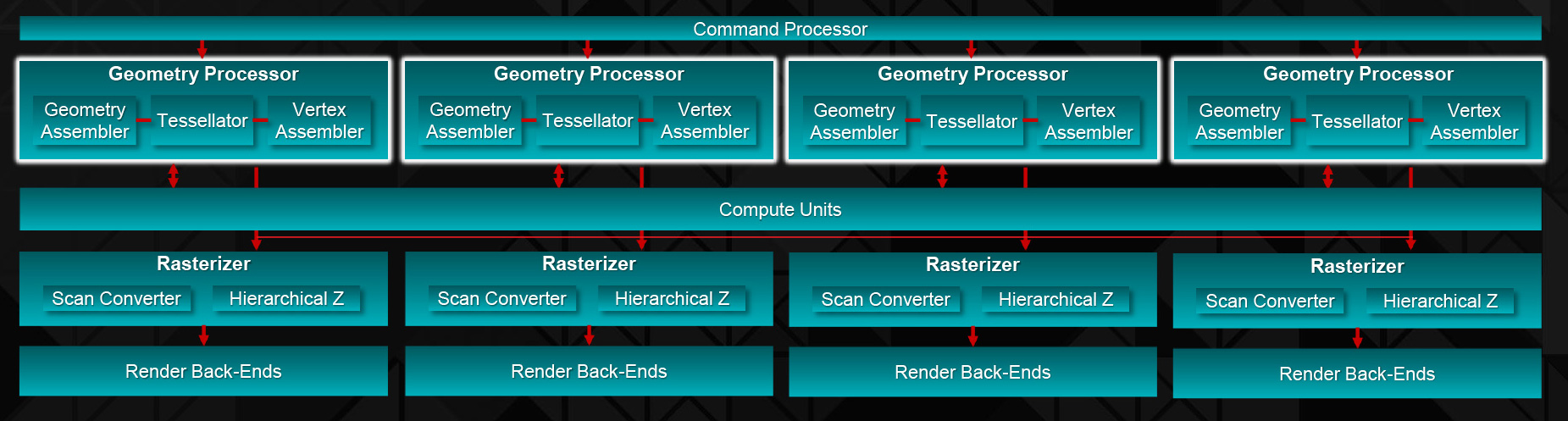
Along those lines, while shading performance is greatly increased over Hawaii, the rest of the front-end is very similar from a raw, theoretical point of view. The geometry processors, which as we mentioned before are organized to 1 per shader engine, just as was the case with Hawaii. With a 1 poly/clock limit here, Fiji has the same theoretical triangle throughput at Hawaii did, with real-world clockspeeds driving things up just a bit over the R9 290X. However as we discussed in our look at the GCN 1.2 architecture, AMD has made some significant under-the-hood changes to the geometry processor design for GCN 1.2/Fiji in order to boost their geometry efficiency, making Fiji’s geometry fornt-end faster and more efficient than Hawaii. As a result the theoretical performance may be unchanged, but in the real world Fiji is going to offer better geometry performance than Hawaii does.
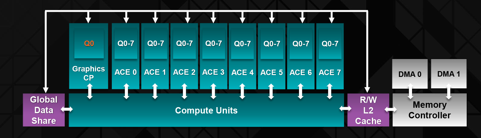
Meanwhile the command processor/ACE structure remains unchanged from Hawaii. We’re still looking at a single graphics command processor paired up with 8 Asynchronous Compute Engines here, and if AMD has made any changes to this beyond what is necessary to support the GCN 1.2 feature set (e.g. context switching, virtualization, and FP16), then they have not disclosed it. AMD is expecting asynchronous shading to be increasingly popular in the coming years, especially in the case of VR, so Fiji’s front-end is well-geared towards the future AMD is planning for.
Moving on, let’s switch gears and talk about the back-end of the processor. There are some significant changes here due to HBM, as to be expected, but there are also some other changes going on as well that are not related to HBM.
Starting with the ROPs, the ROP situation for Fiji remains more or less unchanged from Hawaii. Hawaii shipped with 64 ROPs grouped in to 16 Render Backends (RBs), which at the time AMD told us was the most a 4 shader engine GCN GPU could support. And I suspect that limit is still in play here, leading to Fiji continuing to pack 64 ROPs. Given that AMD just went from 32 to 64 a generation ago, another jump seemed unlikely anyhow (despite earlier rumors to the contrary), but in the end I suspect that AMD had to consider architectural limits just as much as they had to consider performance tradeoffs of more ROPs versus more shaders.
In any case, the real story here isn’t the number of ROPs, but their overall performance. Relative to Hawaii, Fiji’s ROP performance is getting turbocharged for two major reasons. The first is GCN 1.2’s delta color compression, which significantly reduces the amount of memory bandwidth the ROPs consume. Since the ROPs are always memory bandwidth bottlenecked – and this was even more true on Hawaii as the ROP/bandwidth ratio fell relative to Tahiti – anything that reduces memory bandwidth needs can boost performance. We’ve seen this first-hand on R9 285, which with its 256-bit memory bus had no problem keeping up with (and even squeaking past) the 384-bit bus of the R9 280.
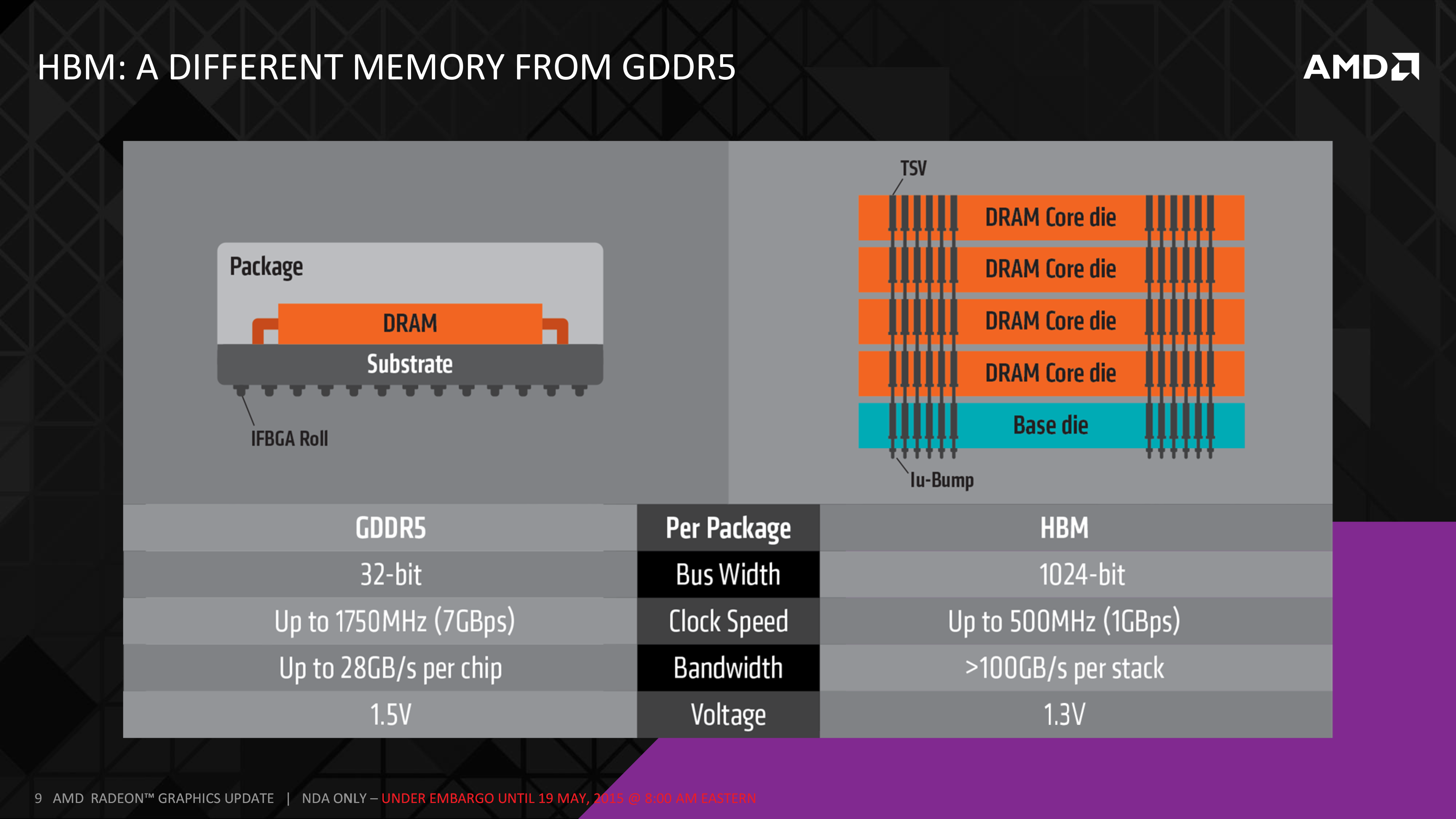
The other factor turbocharging Fiji’s ROPs is of course the HBM. In case GCN 1.2’s bandwidth savings were not enough, Fiji also just flat-out has quite a bit more memory bandwidth to play with. The R9 290X and its 5Gbps, 512-bit memory bus offered 320GB/sec, a value that for a GDDR5-based system has only just been overshadowed by the R9 390X. But with Fiji, the HBM configuration as implemented on the R9 Fury X gives AMD 512GB/sec, an increase of 192GB/sec, or 60%.
Now AMD did not just add 60% more memory bandwidth because they felt like it, but because they’re putting that memory bandwidth to good use. The ROPs would still gladly consume it all, and this doesn’t include all of the memory bandwidth consumed by the shaders, the geometry engines, and the other components of the GPU. GPU performance has long outpaced memory bandwidth improvements, and while HBM doesn’t erase any kind of conceptual deficit, it certainly eats into it. With such a significant increase in memory bandwidth and combined with GCN 1.2’s color compression technology, AMD’s effective memory bandwidth to their ROPs has more than doubled from Hawaii to Fiji, which will go a long way towards increasing ROP efficiency and real-world performance. And even if a task doesn’t compress well (e.g. compute) then there’s still 60% more memory bandwidth to work with. Half of a terabyte-per-second of memory bandwidth is simply an incredible amount to have for such a large pool of VRAM, since prior to this only GPU caches operated that quickly.
Speaking of caches, Fiji’s L2 cache has been upgraded as well. With Hawaii AMD shipped a 1MB cache, and now with Fiji that cache has been upgraded again to 2MB. Even with the increase in memory bandwidth, going to VRAM is still a relatively expensive operation, so trying to stay on-cache is beneficial up to a point, which is why AMD spent the additional transistors here to double the L2 cache. Both AMD and NVIDIA have gone with relatively large L2 caches in this latest round, and with their latest generation color compression technologies it makes a lot of sense; since the L2 cache can store color-compressed tiles, all of a sudden L2 caches are a good deal more useful and worth the space they consume.
Finally, we’ll get to HBM in a more detail in a bit, but let’s take a quick look at the HBM controller layout. With Fiji there are 8 HBM memory controllers, and each HBM controller in turn drives one-half of an HBM stack, meaning 2 controllers are necessary to drive a full stack. And while AMD’s logical diagram doesn’t illustrate it, Fiji is almost certainly wired such that each HBM memory controller is tightly coupled with 8 ROPs and 256KB of L2 cache. AMD has not announced any future Fiji products with less than 4GB of VRAM, so we’re not expecting any parts with disabled ROPs, but if they did that would give you an idea of how things would be disabled.


458 Comments
View All Comments
looncraz - Friday, July 3, 2015 - link
75MHz on a factory low-volting GPU is actually to be expected. If the voltage scaled automatically, like nVidia's, there is no telling where it would go. Hopefully someone cracks the voltage lock and gets to cranking of the hertz.chizow - Friday, July 3, 2015 - link
North of 400W is probably where we'll go, but I look forward to AMD exposing these voltage controls, it makes you wonder why they didn't release them from the outset given they made the claims the card was an "Overclocker's Dream" despite the fact it is anything but this.Refuge - Friday, July 3, 2015 - link
It isn't unlocked yet, so nobody has overclocked it yet.chizow - Monday, July 6, 2015 - link
But but...AMD claimed it was an Overclocker's Dream??? Just another good example of what AMD says and reality being incongruent.Thatguy97 - Thursday, July 2, 2015 - link
would you say amd is now the "geforce fx 5800"sabrewings - Thursday, July 2, 2015 - link
That wasn't so much due to ATI's excellence. It had a lot to do with NVIDIA dropping the ball horribly, off a cliff, into a black hole.They learned their lessons and turned it around. I don't think either company "lost" necessarily, but I will say NVIDIA won. They do more with less. More performance with less power, less transistors, less SPs, and less bandwidth. Both cards perform admirably, but we all know the Fury X would've been more expensive had the 980 Ti not launched where it did. So, to perform arguably on par, AMD is living with smaller margins on probably smaller volume while Nvidia has plenty of volume with the 980 Ti and their base cost is less as they're essentially using Titan X throw away chips.
looncraz - Thursday, July 2, 2015 - link
They still had to pay for those "Titan X throw away chips" and they cost more per chip to produce than AMD's Fiji GPU. Also, nVidia apparently had to not cut down the GPU as much as they were planning as a response to AMD's suspected performance. Consumers win, of course, but it isn't like nVidia did something magical, they simply bit the bullet and undercut their own offerings by barely cutting down the Titan X to make the 980Ti.That said, it is very telling that the AMD GCN architecture is less balanced in relation to modern games than the nVidia architecture, however the GCN architecture has far more features that are going unused. That is one long-standing habit ATi and, now, AMD engineers have had: plan for the future in their current chips. It's actually a bad habit as it uses silicon and transistors just sitting around sucking up power and wasting space for, usually, years before the features finally become useful... and then, by that time, the performance level delivered by those dormant bits is intentionally outdone by the competition to make AMD look inferior.
AMD had tessellation years before nVidia, but it went unused until DX11, by which time nVidia knew AMD's capabilities and intentionally designed a way to stay ahead in tessellation. AMD's own technology being used against it only because it released it so early. HBM, I fear, will be another example of this. AMD helped to develop HBM and interposer technologies and used them first, but I bet nVidia will benefit most from them.
AMD's only possible upcoming saving grace could be that they might be on Samsung's 14nm LPP FinFet tech at GloFo and nVidia will be on TSMC's 16nm FinFet tech. If AMD plays it right they can keep this advantage for a couple generations and maximize the benefits that could bring.
vladx - Thursday, July 2, 2015 - link
Afaik, even though TSMC's GinFet will be 16nm it's a superior process overall to GloFo's 14nm FF so I dount AMD will gain any advantage.testbug00 - Sunday, July 5, 2015 - link
TSMC's FinFET 16nm process might be better than GloFo's own canceled 14XM or whatever they called it.Better than Samsung's 14nm? Dubious. Very unlikely.
chizow - Sunday, July 5, 2015 - link
Why is it dubious? What's the biggest chip Samsung has fabbed? If they start producing chips bigger than the 100mm^2 chips for Apple, then we can talk but as much flak as TSMC gets flak over delays/problems, they still produce what are arguably the world's most advanced seminconductors, right there next to Intel's biggest chips in size and complexity.