AMD Dives Deep On High Bandwidth Memory - What Will HBM Bring AMD?
by Ryan Smith on May 19, 2015 8:40 AM EST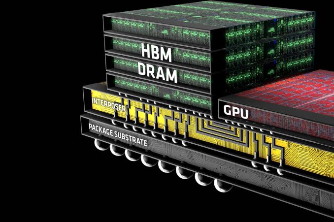
Though it didn’t garner much attention at the time, in 2011 AMD and memory manufacturer Hynix (now SK Hynix) publicly announced plans to work together on the development and deployment of a next generation memory standard: High Bandwidth Memory (HBM). Essentially pitched as the successor to GDDR, HBM would implement some very significant changes in the working of memory in order to further improve memory bandwidth and turn back the dial on memory power consumption.
AMD (and graphics predecessor ATI) for their part have in the last decade been on the cutting edge of adopting new memory technologies in the graphics space, being the first to deploy products based on the last 2 graphics DDR standards, GDDR4, and GDDR5. Consequently, AMD and Hynix’s announcement, though not a big deal at the time, was a logical extension of AMD’s past behavior in continuing to explore new memory technologies for future products. Assuming everything were to go well for the AMD and Hynix coalition – something that was likely, but not necessarily a given – in a few years the two companies would be able to bring the technology to market.
AMD Financial Analyst Day 2015
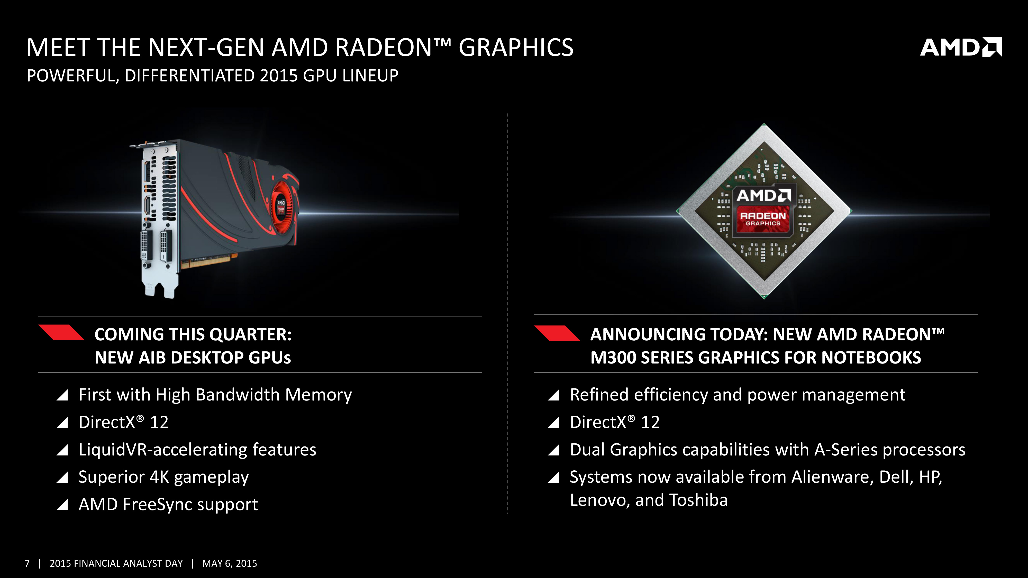
It’s now 4 years later, and successful experimentation has given way to productization. Earlier this month at AMD’s 2015 Financial Analyst day, the company announced that they would be releasing their first HBM-equipped GPU – the world’s first HBM-equipped GPU, in fact – to the retail market this quarter. Since then there have been a number of questions of just what AMD intends to do with HBM and just what it means for their products (is it as big of a deal as it seems?), and while AMD is not yet ready to reveal the details of their forthcoming HBM-equipped GPU, the company is looking to hit the ground running on HBM in order to explain what the technology is and what it can do for their products ahead of the GPU launch later that quarter.
To date there have been a number of presentations released on HBM, including by memory manufactures, the JEDEC groups responsible for shaping HBM, AMD, and even NVIDIA. So although the first HBM products have yet to hit retail shelves, the underpinnings of HBM are well understood, at least inside of engineering circles. In fact it’s the fact that HBM is really only well understood within those technical circles that’s driving AMD’s latest disclosure today. AMD sees HBM as a significant competitive advantage over the next year, and with existing HBM presentations having been geared towards engineers, academia, and investors, AMD is looking to take the next step and reach out to end-users about HBM technology.
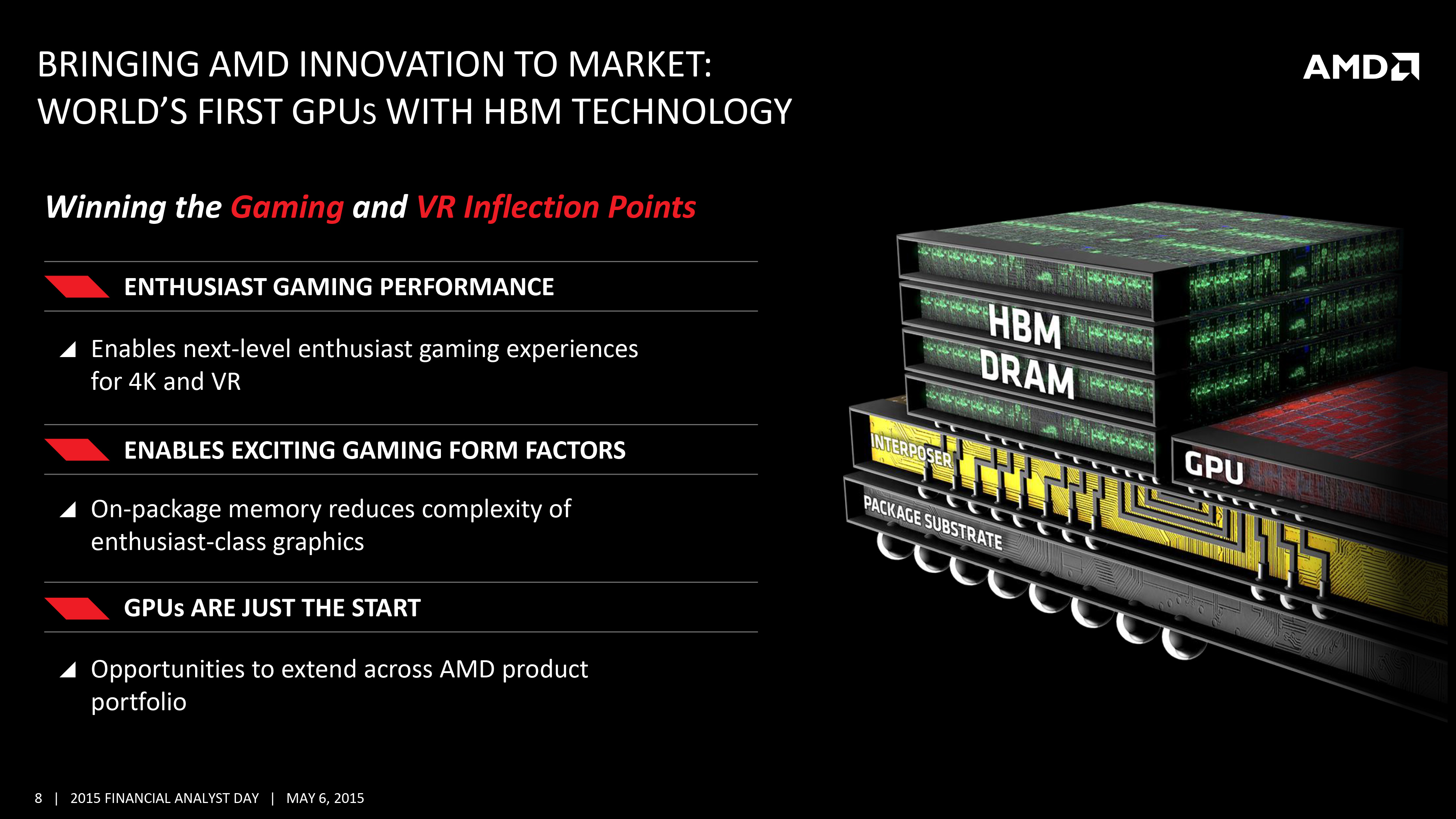
This brings us to the topic of today’s article: AMD’s deep dive disclosure on High Bandwidth Memory. Looking to set the stage ahead of their next GPU launch, AMD is reaching out to technical and gaming press to get the word out about HBM and what it means for AMD’s products. Ideally for AMD, an early disclosure on HBM can help to drum up interest in their forthcoming GPU before it launches later this quarter, but if nothing else it can help answer some burning questions about what to expect ahead of the launch. So with that in mind, let’s dive in.
I'd also like to throw out a quick thank you to AMD Product CTO and Corporate Fellow Joe Macri, who fielded far too many questions about HBM.


163 Comments
View All Comments
chizow - Tuesday, May 19, 2015 - link
Nice article Ryan, I think this gets back to some of the general tech deep dives that a lot of people miss on AT, rather than the obligatory item reviews that I know you guys have to put out as well. Always interesting to read about new and upcoming technology, thanks for the read!This part I think however, on last page needs to be clarified, as it is REALLY important to stay consistent in terminology now that GPU socket and PCB topology is changing:
"By AMD’s own estimate, a single HBM-equipped GPU package would be less than 70mm X 70mm (4900mm2), versus 110mm X 90mm (9900mm2) for R9 290X."
Even by AMD's own slide, that is *PCB area* occupied by either the HBM GPU package, or the GPU + GDDR5 modules. Calling everything a "package" doesn't really fit here and just confuses the issue if we keep the term Package intact, meaning GPU substrate sitting on PCB.
extide - Tuesday, May 19, 2015 - link
No, package is the correct term, as it is a single complete item that attaches to the PCB, including the GPU, RAM, interposer, etc all in one piece. It is not much different than the MCM (Multi Chip Modules) that many manufacturers (Intel for example) have used in the past. Since the memory is all on the package, the PCB area used is the same size as the package itself, in this case.chizow - Tuesday, May 19, 2015 - link
I agree the HBM package terminology is correct, but I'm not referring to that. I'm referring to the reference that the 290X package size is 110mm x 90mm for R9 290X. That's not very clear, because they are counting the *PCB AREA* on the 290X and using it synonymously with Package.It would be more clearly stated if it read something like:
"By AMD’s own estimate, the PCB area occupied by a single HBM-equipped GPU package would be less than 70mm X 70mm (4900mm2), versus 110mm X 90mm (9900mm2) PCB area for R9 290X that includes the GPU package and GDDR5 modules."
gamerk2 - Tuesday, May 19, 2015 - link
How much does the production of the Interposer cost? It's obviously going to eat into AMDs margins, which would imply that unless they sell more product, their profits will actually decline. Likewise, I wonder if that extra cost is going to squeeze them on the low end, where they currently have an advantage.extide - Tuesday, May 19, 2015 - link
Probably on the order of $10/GPU -- not a ton, but enough to be a significant item on the BoM.DanNeely - Tuesday, May 19, 2015 - link
I doubt gen 1 HBM will show up on budget cards; and wouldn't hold my breath on gen 2 or 3 either. For the 4xx generation, they're only putting it on the 490 family. 460-480 are going to remain at GDDR5. HBM will presumably kill off GDDR5 for midlevel cards over the next few years; but unless it becomes as cheap as DDR4 it's not going to be a factor on budget GPUs.SunLord - Tuesday, May 19, 2015 - link
I wonder how this will impact dual gpu cardsKevin G - Tuesday, May 19, 2015 - link
It'd actually make the board design simpler as difficult part, the memory traces, are now all in the interposer. The challenge for a dual GPU designs shifts toward power and cooling.With the board area savings, they could conceptually do a triple GPU card. The problem wouldn't be the designs of such a card but actually getting enough power. Of course they could go out of the PCIe spec and go towards a 525W design for such a triple GPU beast.
testbug00 - Tuesday, May 19, 2015 - link
Naw, they would go for a full water cooled 725W card XD (1W under the electric limits of PCI + 8 + 8 pin iirc) trollololoolololol.don't think anyone would do a triple GPU card for consumers. The scaling is still pretty bad beyond 2 iirc.
Kevin G - Tuesday, May 19, 2015 - link
The wonderful thing about having all the GPUs on a single board is that incorporating a private high speed bus between chips becomes possible to improve scaling. AMD attempted this before with the 4870X2: http://www.anandtech.com/show/2584/3However, it was never really utilized as it was disabled via drivers.
Alternatively, multiple GPU dies and memory could just be placed onto the same the interposer. Having a fast and wide bus between GPU dies would then become trivial. Power consumption and more importantly power density, would not be so trivial.