AMD Dives Deep On High Bandwidth Memory - What Will HBM Bring AMD?
by Ryan Smith on May 19, 2015 8:40 AM EST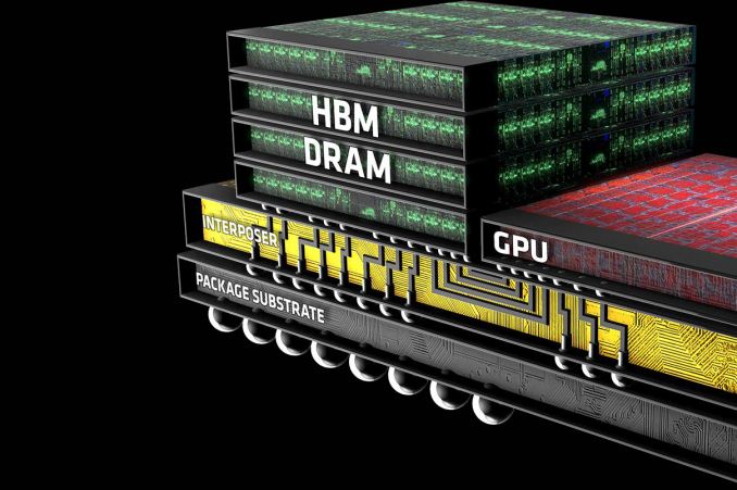
Though it didn’t garner much attention at the time, in 2011 AMD and memory manufacturer Hynix (now SK Hynix) publicly announced plans to work together on the development and deployment of a next generation memory standard: High Bandwidth Memory (HBM). Essentially pitched as the successor to GDDR, HBM would implement some very significant changes in the working of memory in order to further improve memory bandwidth and turn back the dial on memory power consumption.
AMD (and graphics predecessor ATI) for their part have in the last decade been on the cutting edge of adopting new memory technologies in the graphics space, being the first to deploy products based on the last 2 graphics DDR standards, GDDR4, and GDDR5. Consequently, AMD and Hynix’s announcement, though not a big deal at the time, was a logical extension of AMD’s past behavior in continuing to explore new memory technologies for future products. Assuming everything were to go well for the AMD and Hynix coalition – something that was likely, but not necessarily a given – in a few years the two companies would be able to bring the technology to market.
AMD Financial Analyst Day 2015
It’s now 4 years later, and successful experimentation has given way to productization. Earlier this month at AMD’s 2015 Financial Analyst day, the company announced that they would be releasing their first HBM-equipped GPU – the world’s first HBM-equipped GPU, in fact – to the retail market this quarter. Since then there have been a number of questions of just what AMD intends to do with HBM and just what it means for their products (is it as big of a deal as it seems?), and while AMD is not yet ready to reveal the details of their forthcoming HBM-equipped GPU, the company is looking to hit the ground running on HBM in order to explain what the technology is and what it can do for their products ahead of the GPU launch later that quarter.
To date there have been a number of presentations released on HBM, including by memory manufactures, the JEDEC groups responsible for shaping HBM, AMD, and even NVIDIA. So although the first HBM products have yet to hit retail shelves, the underpinnings of HBM are well understood, at least inside of engineering circles. In fact it’s the fact that HBM is really only well understood within those technical circles that’s driving AMD’s latest disclosure today. AMD sees HBM as a significant competitive advantage over the next year, and with existing HBM presentations having been geared towards engineers, academia, and investors, AMD is looking to take the next step and reach out to end-users about HBM technology.
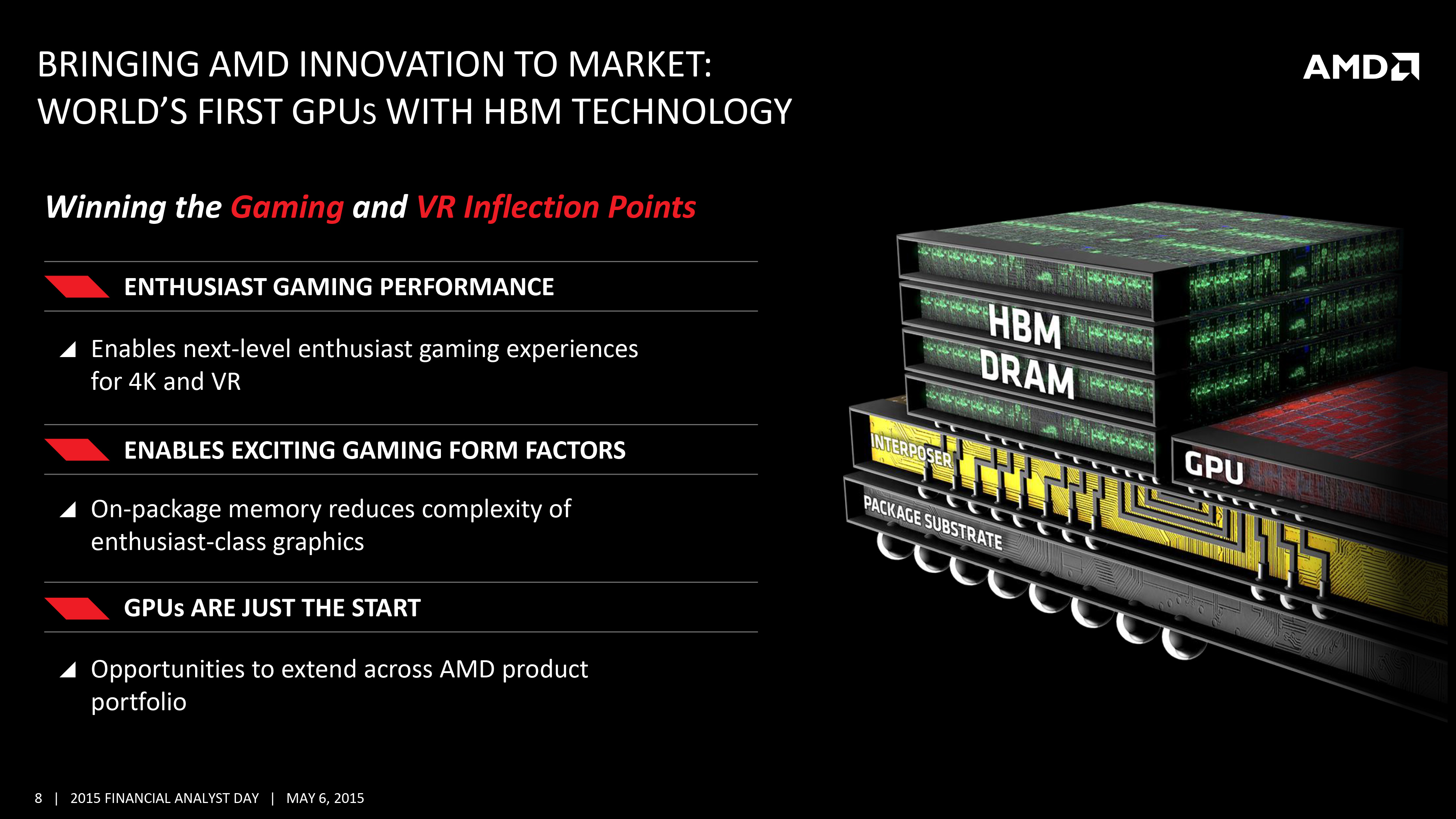
This brings us to the topic of today’s article: AMD’s deep dive disclosure on High Bandwidth Memory. Looking to set the stage ahead of their next GPU launch, AMD is reaching out to technical and gaming press to get the word out about HBM and what it means for AMD’s products. Ideally for AMD, an early disclosure on HBM can help to drum up interest in their forthcoming GPU before it launches later this quarter, but if nothing else it can help answer some burning questions about what to expect ahead of the launch. So with that in mind, let’s dive in.
I'd also like to throw out a quick thank you to AMD Product CTO and Corporate Fellow Joe Macri, who fielded far too many questions about HBM.


163 Comments
View All Comments
testbug00 - Tuesday, May 19, 2015 - link
Name long term good relationships that Nvidia has had with other companies in the industry. Besides their board partners. You could argue TSMC either way. Otherwise, I'm getting nothing. They recently have a relationship with IBM that could become long term. It is entirely possible I'm just missing the companies they partner with that are happy with their partnership in the semi-conductor industry.Compared to IBM, TSMC, SK Hynix, and more.
ImSpartacus - Tuesday, May 19, 2015 - link
Can we have an interview with Joe Macri? He seems like a smart fella if he was the primary reference for this article.wnordyke - Tuesday, May 19, 2015 - link
This analysis does not discuss the benefits of the base die? The base die contains the memory controller and a data serializer. The architecture of moving the memory controller to the base die simplifies the design and removes many bottlenecks. The Base die is large enough to support a large number of circuits. (#1 memory controller, #2 Cache, #3 data processing)The 4096 wires is a large number and 4096 I/O buffers is a large number. The area of 4096 I/O buffers on the GPU die is expensive, and this expense is easily avoided by placing the memory controller on the base die. The 70% memory Bus efficiency is idle bandwidth, and this idle data does not need to be sent back to the GPU. The 4096 Interposer signals reduces to (4096 * 0.7 = 2867) saving 1,229 wires + I/O buffers.
A simple 2 to 1 serializer would reduces down to (2867 * 0.50 = 1432). The Interposer wires are short enough to avoid the termination resistors for a 2GHz signal. Removing the termination resistors is top of the list to saving power, the second on the list to save power is to minimize the Row Activate.
takeship - Tuesday, May 19, 2015 - link
So am I correct in assume then that the 295x2 equivalent performance numbers for Fiji leaked months ago are for the dual gpu variant? It concerns me that at no point in this write up did AMD even speculate what the performance inc with HBM might be.dew111 - Tuesday, May 19, 2015 - link
Why is everyone concerned about the 4GB limit in VRAM? A few enthusiasts might be disappointed, but for anyone who isn't using multiple 4k monitors, 4GB is just fine. It might also be limiting in some HPC workloads, but why would any of us consumers care about that?chizow - Wednesday, May 20, 2015 - link
I guess the concern is that people were expecting AMD's next flagship to pick up where they left off on the high-end, and given how much AMD has touted 4K, that would be a key consideration. Also, there are the rumors this HBM part is $850 to create a new AMD super high-end, so yeah, if you're going to say 4K is off the table and try to sell this as a super premium 4K part, you're going to have a hard sell as that's just a really incongruent message.In any case, AMD says they can just driver-magic this away, which is a recurring theme for AMD, so we will see. HBM's main benefits are VRAM to GPU transfers, but anything that doesn't fit in the local VRAM are still going to need to come from System RAM or worst, local storage. Textures for games are getting bigger than ever...so yeah not a great situation to be stuck at 4GB for anything over 1080p imo.
zodiacfml - Tuesday, May 19, 2015 - link
Definitely for their APUs and mobile. Making this first on GPUs helps recover the R&d without the volume scale.SolMiester - Tuesday, May 19, 2015 - link
Do the R9 290\x really perform that much better with OC memory on the cards? I didnt think AMD was ever really constrained by bandwidth, as they usually always had more on their generation of cards.Consequently, I dont see 390\x being that much competition to Titan X
Intel999 - Tuesday, May 19, 2015 - link
Thanks SolMiester,You have done an excellent job of displaying your level of intelligence. I don't think the New York Giants will provide much competition to the rest of the NFL this year. I won't support my prediction with any facts or theories just wanted to demonstrate that I am not a fan of the Giants.
BillyHerrington - Tuesday, May 19, 2015 - link
Since HBM are owned by AMD & Hynix, does other company (nvidia, etc) have to pay AMD in order to use HBM tech ?