Intel & Cray Land Contract for 2 Dept. of Energy Supercomputers
by Ryan Smith on April 9, 2015 5:30 PM EST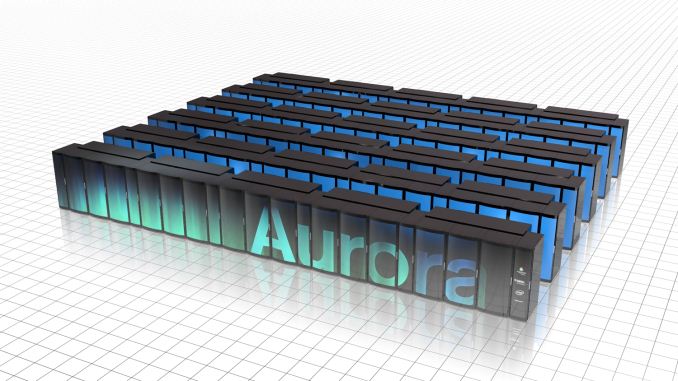
Late last year the United States Department of Energy kicked off the awards phase of their CORAL supercomputer upgrade project, which would see three of the DoE’s biggest national laboratories receive new supercomputers for their ongoing research work. The first two supercomputers, Summit and Sierra, were awarded to the IBM/NVIDIA duo for Oak Ridge National Laboratory and Lawrence Livermore National Laboratory respectively. Following up on that, the final part of the CORAL program is being awarded today, with Intel and Cray receiving orders to build 2 new supercomputers for Argonne National Laboratory.
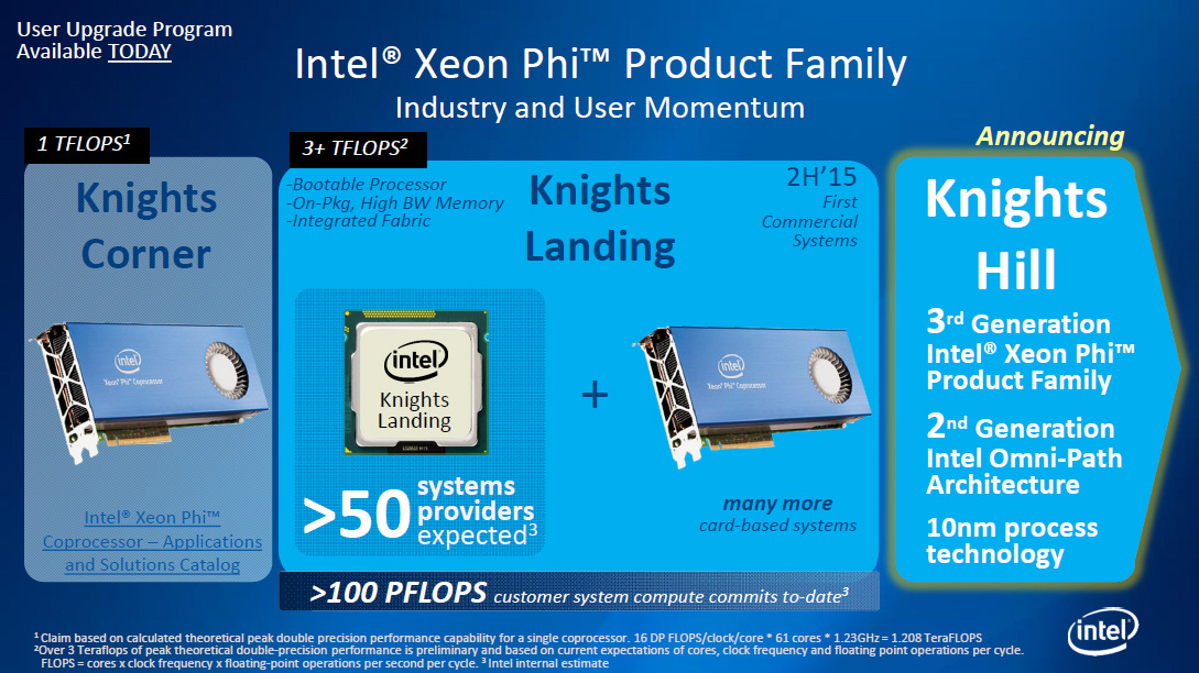
The flagship of these two computers is Aurora, a next-generation Cray “Shasta” supercomputer that is scheduled for delivery in 2018. Designed to deliver 180 PetaFLOPS of peak compute performance, Aurora will be heavily leveraging Intel’s suite of HPC technologies. Primarily powered by a future version of Intel’s Xeon Phi accelerators – likely the 10nm-fabbed Knights Hill – Aurora will be combining the Xeon Phi with Intel’s Xeon CPUs (Update: Intel has clarified that the Xeons are for management purposes only), an unnamed Intel developed non-volatile memory solution, and Intel’s high-speed and silicon photonics-driven Omni-Path interconnect technology. Going forward, Intel is calling this future setup their HPC scalable system framework.
At 180 PFLOPS of performance, Aurora will be in the running for what will be the world’s fastest supercomputer. Whether it actually takes the crown will depend on where exactly ORNL’s Summit supercomputer ends up – it’s spec’d for between 150 PFLOPS and 300 PFLOPS – with Aurora exceeding the minimum bounds of that estimate. All told this makes Aurora 18 times faster than its predecessor, the 10 PFLOPS Mira supercomputer. Meanwhile Aurora’s peak power consumption of 13MW is also 2.7 times Mira’s, which works out to an overall increase in energy efficiency of 6.67x.
| US Department of Energy CORAL Supercomputers | ||||||
| Aurora | Theta | Summit | Sierra | |||
| CPU Architecture | Intel Xeon (Management Only) |
Intel Xeon (Management Only) |
IBM POWER9 | IBM POWER9 | ||
| Accelerator Architecture | Intel Xeon Phi (Knights Hill?) | Intel Xeon Phi (Knights Landing) | NVIDIA Volta | NVIDIA Volta | ||
| Performance (RPEAK) | 180 PFLOPS | 8.5 PFLOPS | 150 - 300 PFLOPS | 100+ PFLOPS | ||
| Power Consumption | 13MW | 1.7MW | ~10MW | N/A | ||
| Nodes | N/A | N/A | 3,400 | N/A | ||
| Laboratory | Argonne | Argonne | Oak Ridge | Lawrence Livermore | ||
| Vendor | Intel + Cray | Intel + Cray | IBM | IBM | ||
The second of the supercomputers is Theta, which is a much smaller scale system intended for early production system for Argonne, and is scheduled for delivery in 2016. Theta is essentially a one-generation sooner supercomputer for further development, based around a Cray XC design and integrating Intel Xeon processors along with Knights Landing Xeon Phi processors. Theta in turn will be much smaller than Aurora, and is scheduled to deliver a peak performance of 8.5 PFLOPS while consuming 1.7MW of power.
The combined value of the contract for the two systems is over $200 million, the bulk of which is for the Aurora supercomputer. Interestingly the prime contractor for these machines is not builder Cray, but rather Intel, with Cray serving as a sub-contractor for system integration and manufacturing. According to Intel this is the first time in nearly two decades that they have been awarded the prime contractor role in a supercomputer, their last venture being ASCI Red in 1996. Aurora in turn marks the latest in a number of Xeon Phi supercomputer design wins for Intel, joining existing Intel wins such as the Cori and Trinity supercomputers. Meanwhile for partner Cray this is also the first design win for their Shasta family of designs.
Finally, Argonne and Intel have released a bit of information on what Aurora will be used for. Among fields/tasks planned for research on Aurora are: battery and solar panel improvements, wind turbine design and placement, improving engine noise & efficiency, and biofuel research, including more effective disease control for biofuel crops.
Source: Intel


35 Comments
View All Comments
testbug00 - Friday, April 10, 2015 - link
His question was more about Intel supporting it. How fast Gen4 is doesn't matter if Intel doesn't use it at all. Broadwell offers a total of 12 PCI 2.0 lanes, 2x4, 4x1. That drops the performance of a 980 9% at 1440p. Now, those are all laptop parts so far, so, the PCI implementation there is likely for maximum power saving. Hopefully desktop chips bring more.http://www.anandtech.com/show/8814/intel-releases-...
Zotamedu - Thursday, April 16, 2015 - link
That's Broadwell-U, the low power SOC version with a maximum TDP of 28 W. They are not comparable with the larger Haswell or upcoming Skylake chips. Skylake will have even more total bandwidth than Haswell because they will increase the bandwidth the the PCH when they update to DMI 3.0. So that's PCIe 3.0 x16 from the CPU and double the bandwidth to PCH to 40 Gb/s. PCIe 4.0 is expected to show up in Skylake-E. Bandwidth to GPUs isn't that much of a bottleneck currently. PCIe 3.0 x16 is enough for most dual GPU systems today and for the larger builds, there's always the s2011 platforms with more lanes. A doubling of bandwidth with PCIe 4.0 will make sure bandwidth is not a problem. They are moving faster than the GPU manufacturers can.Why would Intel invest in a product designed by Nvidia for HPC use? Nvlink is not made to replace PCIe in gaming computers. It's designed for HPC and even there it's a niche product.
mehrotrasc - Friday, April 10, 2015 - link
Congratulations to all members of the team for excellent product which will lead to many breakthrough real time applications...dahippo - Saturday, April 11, 2015 - link
Can I dropp a a-bomb faster or is it wrong department :)JoJoman88 - Saturday, April 11, 2015 - link
Sorry Testbug, it was a joke. I always get a kick out of people who think stuff like this would apply to their regular PC. Guess it was my inside joke then.