NVIDIA Tegra X1 Preview & Architecture Analysis
by Joshua Ho & Ryan Smith on January 5, 2015 1:00 AM EST- Posted in
- SoCs
- Arm
- Project Denver
- Mobile
- 20nm
- GPUs
- Tablets
- NVIDIA
- Cortex A57
- Tegra X1
Final Words
With the Tegra X1, there have been a great deal of changes when compared to Tegra K1. We see a move from Cortex A15 to A57 on the main cluster, and a move from a single low power Cortex A15 to four Cortex A53s which is a significant departure from previous Tegra SoCs. However, the CPU design remains distinct from what we see in SoCs like the Exynos 5433, as NVIDIA uses a custom CPU interconnect and cluster migration instead of ARM’s CCI-400 and global task scheduling. Outside of these CPU changes, NVIDIA has done a great deal of work on the uncore, with a much faster ISP and support for new codecs at high resolution and frame rate, along with an improved memory interface and improved display output.
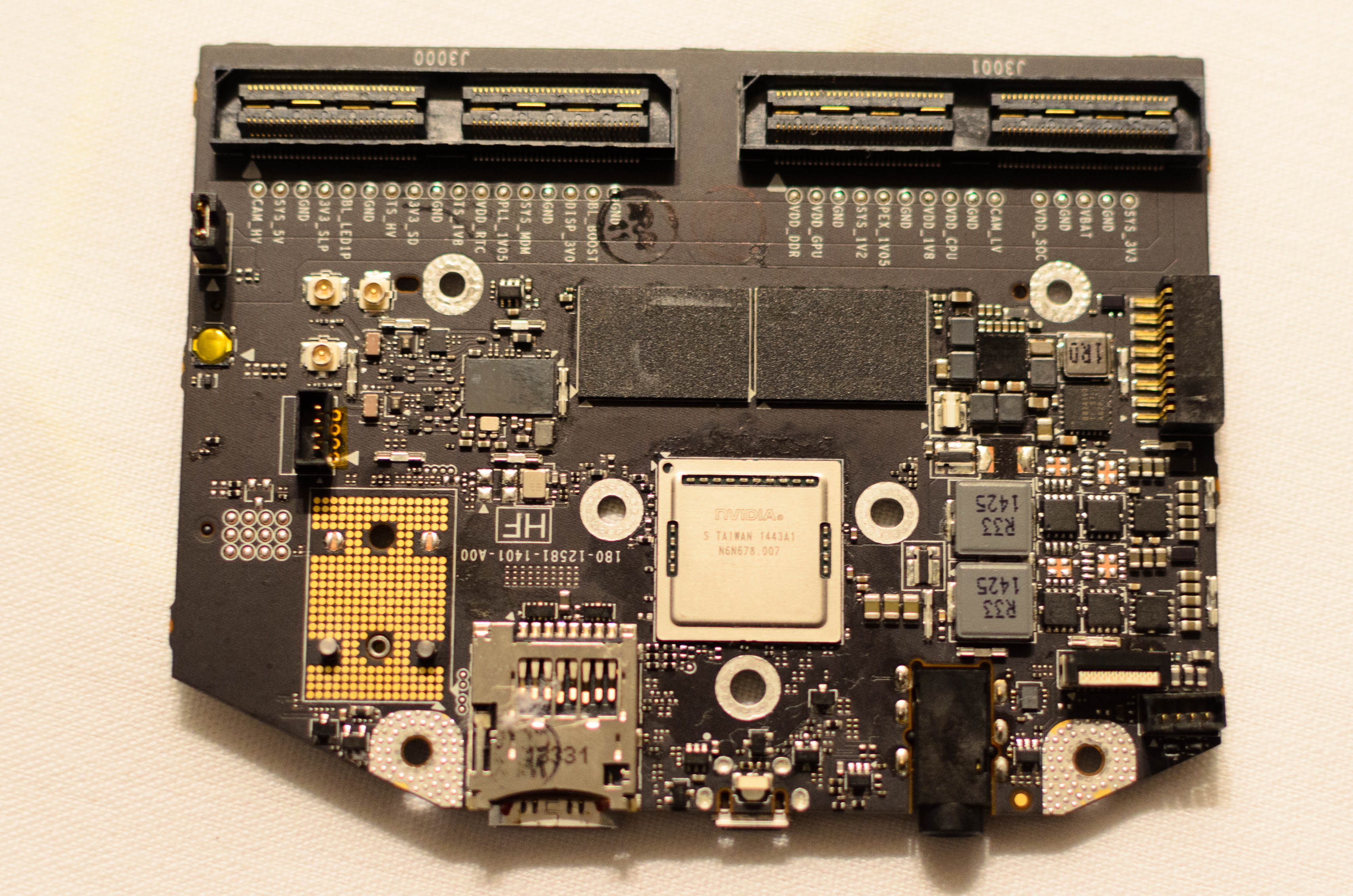
Tegra X1 Reference Platform
Outside of CPU, the GPU is a massive improvement with the move to Maxwell. The addition of double-speed FP16 support for the Tegra X1 helps to improve performance and power efficiency in applications that will utilize FP16, and in general the mobile-first focus on the architecture makes for a 2x improvement in performance per watt. While Tegra K1 set a new bar for mobile graphics for other SoC designers to target, Tegra X1 manages to raise the bar again in a big way. Given the standards support of Tegra X1, it wouldn’t be a far leap to see more extensive porting of games to a version of SHIELD Tablet with Tegra X1.
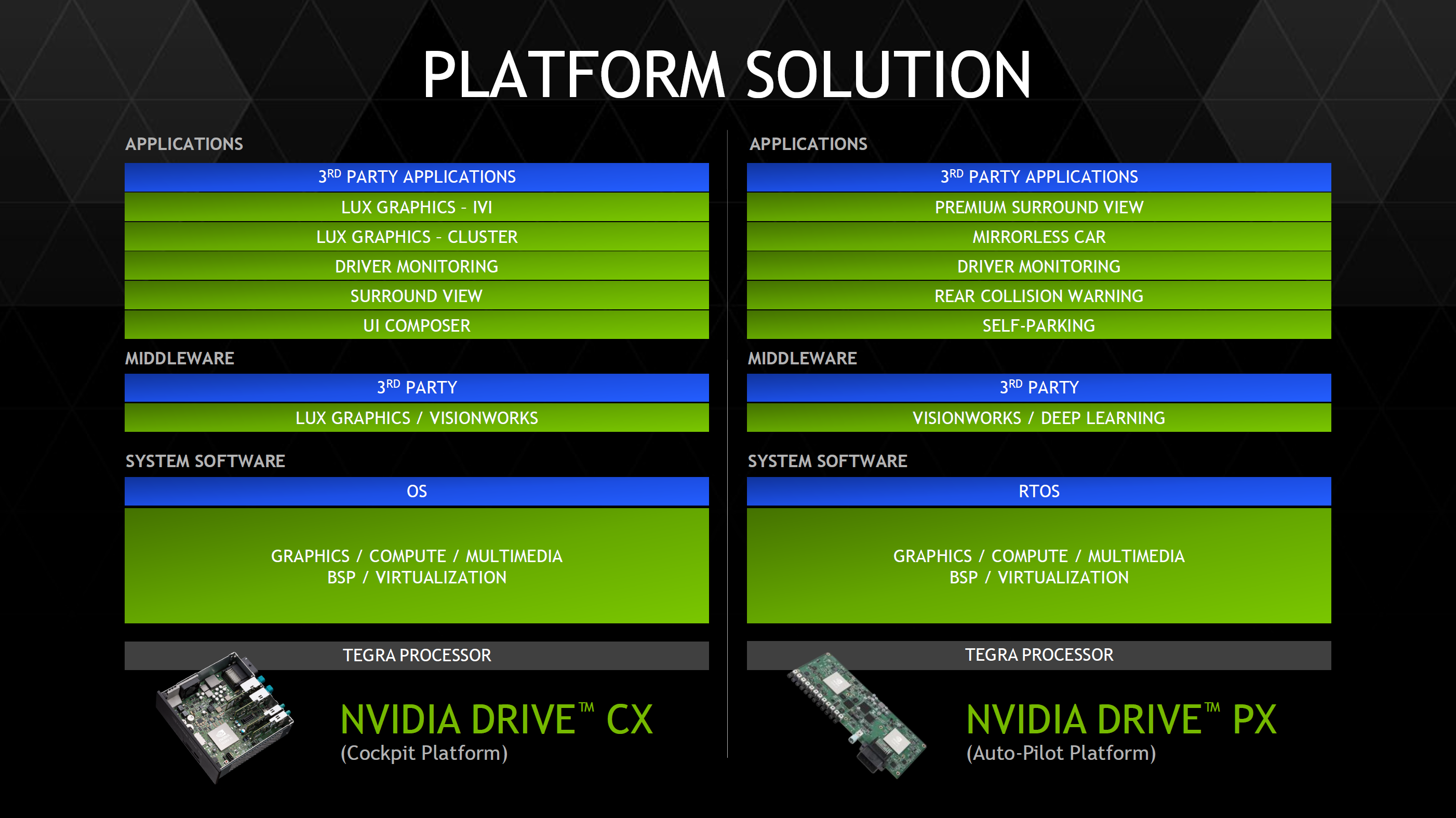
NVIDIA has also made automotive applications a huge focus in Tegra X1 in the form of DRIVE CX, a cockpit computing platform, and DRIVE PX, an autopilot platform. Given the level of integration and compute present in both DRIVE CX and PX, there seems to be a significant amount of value in NVIDIA’s solutions. However, it remains to be seen whether OEMs will widely adopt these solutions as car manufacturers can take multiple years to implement a new SoC. Compared to the 3-4 month adoption rate of an SoC in a phone or tablet, it's hard to pass any judgment on whether or not NVIDIA's automotive endeavors will be a success.
Overall, Tegra X1 represents a solid improvement over Tegra K1, and now that NVIDIA has shifted their GPU architectures to be targeted at mobile first, we’re seeing the benefits that come with such a strategy. It seems obvious that this would be a great SoC to put in a gaming tablet and a variety of other mobile devices, but it remains to be seen whether NVIDIA can get the design wins necessary to make this happen. Given that all of the high-end SoCs in the Android space will be shipping with A57 and A53 CPUs, the high-end SoC space will see significant competition once again.


194 Comments
View All Comments
chizow - Monday, January 5, 2015 - link
Nvidia is only catching up on process node, because what they've shown is when comparing apples to apples:1) They have a much faster custom 64-bit CPU (A8X needed 50% more CPU to edge Denver K1)
2) They have a much faster GPU architecture (A8X also needed 50% more GPU cores to edge Denver K1, but get destroyed by Tegra X1 on the same 20nm node).
As we can see, once it is an even playing field at 20nm, A8X isn't going to be competitive.
GC2:CS - Monday, January 5, 2015 - link
Thy just postponed their "much faster custom 64-bit CPU" in favor of off the shelf design and compared to A8X is much higher clocked.A8X has just 33% percent more "cores" than k1 and aggain the GXA6850 GPU is probably miles under ~1Ghz clockspeed that nvidia targets.
And what's wrong with using a wider CPU/GPU ?
And yeah Tegrax1 is up to 2x faster than A8X, but considering it also runs at the same power as K1, it is not a lot more efficient.
chizow - Monday, January 5, 2015 - link
How do you get only 33% for A8X? A8 = 2 core, Denver K1 = 2 core, A8X = 3 core. 1/2 = 50% increase.Same for A8X over A8. GPU cores went from 4 to 6, again, 2/4 = 50% increase. Total transistors went from 2Bn to 3Bn, again 50% increase.
In summary, Apple fully leveraged 20nm advantage to match Denver K1 GPU and edge in CPU (still losing in single-core) using a brute-force 50% increase in transistors and functional units.
Obviously they won't be able to pull the same rabbit out of the hat unless they go to FinFet early, which is certainly possible, but then again, its not really a magic trick when you pay a hefty premium for early access to the best node is it?
Bottomline is Nvidia is doing more on the same process node as Apple, simple as that, and that's nothing to be ashamed of from an engineering standpoint.
GC2:CS - Monday, January 5, 2015 - link
A8X got 8 GPU clusetrs. And I still can't get your idea, you think that A8X is worse because it's brute force ~ 50% faster ? Yeah it is brute force, but I don't know how can you preceive that as a bad thing.They will certainly try to push finfet and rather hard I think.
And how can you say that nvidia is doing more on the same node while boasting how apple is the one who is doing more and how it's bad just above ?
chizow - Monday, January 5, 2015 - link
Wow A8X is 8 clusters and doesn't even offer a 100% increase over A8? Even worst than I thought, I guess I missed that update at some point over the holiday season.The point is that in order to match the "disappointing" Denver K1, Apple had to basically redouble their efforts to produce a massive 3Bn transistor SoC while fully leveraging 20nm. You do understand that's really not much of an accomplishment when you are on a more advanced process node right?
Sure Apple may push FinFET hard, but from everything I've read, FinFET will be more widely available for ramp compared to the problematic 20nm, which was always limited capacity outside of the premium allocation Apple pushed for (since they obviously needed it to distinguish their otherwise unremarkable SoCs).
It should be obvious why I am saying Nvidia is doing more on the same process node, because when you compare apple to Apples, Nvidia's chip on the 28nm node is more than competitive with the 20nm Apple chips, and when both are on 20nm, its going to be no contest in Nvidia's favor.
Logical conclusion = Nvidia is doing more on the same process node, ie. outperforming their competition when the playing field is leveled.
lucam - Tuesday, January 6, 2015 - link
Chizow the more I read and the more I laugh. You compare clusters with cores they have different technologies and you still state this crap. Maybe would be better to compare how much both of them are capable in term of of GFLOPS at same frequency? This is count. Regarding your absurd discussion of processing node, since the Nvidia chip is so efficient, I look forward to see it in smartphones.aenews - Saturday, January 24, 2015 - link
The A8X isn't on any phones either. In fact, they left it out of both iPhones AND the iPad Mini.And take in mind, even the Qualcomm Snapdragon 805 had few design wins... only the Kindle Fire HDX for tablets. They scored two major phones (Nexus 6 and Note 4) but the other manufacturers haven't used it.
squngy - Monday, January 5, 2015 - link
He did not say it is worse, his whole point is that Apple most likely will not be able to do the same thing again.tipoo - Tuesday, May 17, 2016 - link
Core counts are irrelevant across GPU architectures, they're just different ways of doing something.If someone gets to the same power draw, performance, and die size with 100 cores as someone else does with 10, what does it matter?
Jumangi - Monday, January 5, 2015 - link
Uh the A8 is an actual product that exists and wait for it you can actually BUY a product with it in there. This is another mobile paper launch by Nvidia with the consumer having no idea when or where it will actually be. The only thing real enthusiasts should care about is the companies that can actually deliver parts people can actually use. Nvidia still has a loooong ways to go in that department. Paper specs mean shit.