The NVIDIA GeForce GTX 980 Review: Maxwell Mark 2
by Ryan Smith on September 18, 2014 10:30 PM ESTSynthetics
As always we’ll also take a quick look at synthetic performance. These tests mainly serve as a canary for finding important architectural changes, and with the exception of pixel throughput we are not expecting any major changes for GTX 980 and GM204.
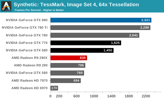
GM204 is designed to have an ever-so-slightly higher triangle throughput rate than GK110 – 16 tris/clock versus 15 tris/clock, and sure enough the GTX 980 comes out on top in TessMark, slightly edging out the GTX 780 Ti. The difference is only very slight here, and though GM204 should be a bit more powerful than GK110 in practice it’s a dead heat.
Moving on, we have our 3DMark Vantage texture and pixel fillrate tests, which present our cards with massive amounts of texturing and color blending work. These aren’t results we suggest comparing across different vendors, but they’re good for tracking improvements and changes within a single product family.
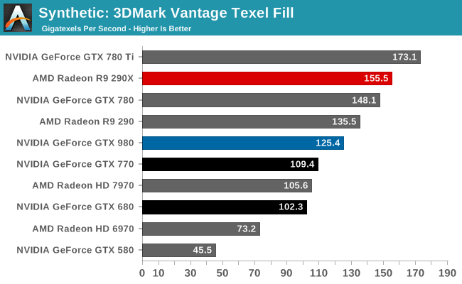
Beginning with Maxwell NVIDIA reduced their texture-to-compute ratio from 12:1 to 16:1. As a result of this change Maxwell GPUs have fewer texture units than comparable Kepler GPUs. Compounding this effect is the fact that Maxwell CUDA cores are more efficient than Kepler CUDA cores, leading to NVIDIA placing fewer cores overall and further reducing the texture fill rate.
As a result the GTX 980 is not texture fillrate competitive with any of the GK110 cards. It is competitive with the GK104 cards, but only because these cards had the same number of texture units at 128. NVIDIA has told us that they believe this new ratio is a better fit for modern workloads, and judging from the performance we’re seeing elsewhere it would appear that NVIDIA is right.
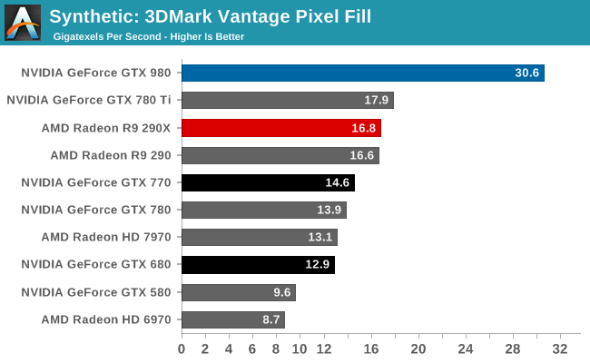
On the other hand, thanks to NVIDIA’s newer 3rd generation delta color compression technology, our 3DMark pixel fillrate performance is through the roof. GTX 980 comes very close to doubling the throughput of our GK110 cards and more than doubles the throughput of the GK104 cards, reflecting the fact that it has 64 ROPs and more importantly has the available bandwidth to put them to good use.
This benchmark in a nutshell is why NVIDIA can deliver chart-topping performance despite having only 2/3rds the memory bandwidth of GTX 780 Ti. By improving their color compression to this point, NVIDIA can significantly reduce their memory bandwidth requirements Maxwell 2, allowing them to do more with less. In real games the result won’t be anywhere near this remarkable since this is a pure pixel fillrate test, but it goes to show that NVIDIA has been able to expand their effective memory bandwidth in concert with their ROP and shader performance improvements.


274 Comments
View All Comments
Frenetic Pony - Friday, September 19, 2014 - link
This is the most likely thing to happen, as the transition to 14nm takes place for intel over the next 6 months those 22nm fabs will sit empty. They could sell capacity at a similar process to TSMC's latest while keeping their advantage at the same time.nlasky - Friday, September 19, 2014 - link
Intel uses the same Fabs to produce 14nm as it does to produce 22nmlefty2 - Friday, September 19, 2014 - link
I can see Nvidia switching to Intel's 14nm, however Intel charges a lot more than TSMC for it's foundry services (because they want to maintain their high margins). That would mean it's only economical for the high end cardsSeanJ76 - Friday, September 19, 2014 - link
What a joke!!!! 980GTX doesn't even beat the previous year's 780ti??? LOL!! Think I'll hold on to my 770 SC ACX Sli that EVGA just sent me for free!!Margalus - Friday, September 19, 2014 - link
uhh, what review were you looking at? or are you dyslexic and mixed up the results between the two cards?eanazag - Friday, September 19, 2014 - link
Nvidia would get twice as many GPUs per wafer on a 14nm process than 28nm. Maxwell at 14nm would blow Intel integrated and AMD out of the water in performance and power usage.That simply isn't the reality. Samsung has better than 28nm processes also. This type of partnership would work well for Nvidia and AMD to partner with Samsung on their fabs. It makes more sense than Intel because Intel views Nvidia as a threat and competitor. There are reasons GPUs are still on 28nm and it is beyond process availability.
astroidea - Friday, September 19, 2014 - link
They'd actually get four times more since you have to considered the squared area. 14^2*4=28^2emn13 - Saturday, September 20, 2014 - link
Unfortunately, that's not how it works. A 14nm process isn't simply a 28nm process scaled by 0.5; different parts are scaled differently, and so the overall die area savings aren't that simple to compute.In a sense, the concept of a "14nm" process is almost a bit of a marketing term, since various components may still be much larger than 14nm. And of course, the same holds for TSMC's 28nm process... so a true comparison would require more knowledge that you or I have, I'm sure :-) - I'm not sure if intel even releases the precise technical details of how things are scaled in the first place.
bernstein - Friday, September 19, 2014 - link
no because intel is using their 22nm for haswell parts... the cpu transition ends in a year with the broadwell xeon-ep... at which point almost all the fabs will either be upgraded or upgrading to 14nm and the rest used to produce chipsets and other secondary die'snlasky - Saturday, September 20, 2014 - link
yes but they use the same fabs for both processes