An Introduction to Semiconductor Physics, Technology, and Industry
by Joshua Ho on October 9, 2014 3:00 PM EST- Posted in
- Semiconductors
- CMOS
- Physics
- Industry
- Technology
Interconnects
Finally, it’s time to talk about what lies ahead. One thing we haven’t talked about yet are the pressing issues of the near future. For example, there are major issues looming with interconnect delay that haven’t been solved yet. As we discussed in BEOL processing, the current system of wiring these metal layers uses copper with a dielectric in between the wires with a tantalum/tantalum nitride cap to support the next layer. However, the smaller the wires get, the worse electron mobility becomes.
This is roughly analogous to the issues that we see in the front end of line, which saw decreasing drive current for the same reasons. Combined with the capacitance produced between wires, there is dramatically increasing RC time delay in the connections made between transistors that hurts performance due to lower peak clock speeds. Ultimately, progress can only be made on this end by using lower k dielectrics and lower resistance materials to drive down both resistance and unwanted capacitance in these circuits.
Next Generation Lithography
There’s still more to talk about though. While we’ve managed to stretch 193mm immersion lithography further than anyone ever imagined, 10 nanometers is likely to be the end of the road for 193nm. Here, the future is unclear. Realistically, it seems that there are only a few techniques that will be viable at the next level. These include extreme ultraviolet lithography (EUVL), nanoimprint lithography, and electron beam lithography. Let's go over each one to try and understand what challenges are coming and which option may be the best in the long run.
EUV
On the surface, EUV is a relatively straight progression of the current 193i deep-UV (DUV) technology and should deliver the significant jump needed to advance lithography beyond 10 nanometer feature sizes. While this seems easy enough, there are a large number of issues that crop up from such a short wavelength (~13nm) of light.
First, the EUV light source itself is no longer a laser in most cases. This means that the energy efficiency of the light source is extremely low compared to current 193nm excimer lasers, and as a result an enormous amount of energy has to be used to generate an incoherent light source that is then filtered to only produce EUV.
Second, EUV is strongly absorbed by almost all matter. This means that the lithography must take place in a vacuum, which rules out techniques such as immersion lithography to further resolution enhancements. By using a strong vacuum for lithography, the amount of wafers that can be processed per hour drops dramatically as vacuuum chucks can no longer be used to hold the wafer, and the electrostatic chucks used must be heated to a stable temperature with a sacrificial wafer. Also, keeping the wafer heating from the EUV exposure becomes a significant issue because the immersion fluid that once cooled the wafer cannot be used.
In addition, it's impossible to use transmissive lenses because of this same issue. As a result, mirrors must be used to focus and reflect the EUV light on to the target. There are potential issues with EUV damaging the mirrors in the optical system, and in order to reflect the EUV light all of the mirrors and the photomask have to be coated with multiple layers that use interference effects to maximize reflected light. This also means that even minor defects in a photomask can result in an unusable photomask, as seen in the photo below.
Buried Defect on EUV Mask Blank / Guiding light / CC BY SA
Unfortunately, these defects cannot be seen using an electron microscope. In order to see these defects, an EUV microscope must be used. Outside of these challenges, EUV itself intrinsically has multiple issues that reduce resolution in some unexpected ways. First, shot noise becomes a serious issue. What this means is that it's fundamentally impossible to completely control the number of photons that are released into the photoresist. This means that the lines drawn by an EUV can be unacceptably rough unless enough photons are used to ensure that shot noise is statistically insignificant, but this only increases the power requirements for EUV lithography. To make things worse, by increasing the amount of exposure to the photoresist the material can be damaged by the sheer intensity of the heating effect of EUV.
Finally, because EUV is so energetic, it is a form of ionizing radiation. This means that when EUV light is absorbed by a molecule, electrons can be liberated. Unfortunately, this adds yet another source of uncertainty and also decreases resolution because the generated photoelectrons move randomly through the photoresist. In effect, all of these issues reduce the true resolution of EUV to somewhere around the 15-19nm feature size for a single exposure. In order to even get to 10nm and below, double patterning is required to reach the resolution necessary.
In short, the resolution gain from current 193nm technology is relatively small compared with the enormous expense and new design challenges. Based on how many delays have occurred with the introduction of EUV lithography, it may mean that a radically new system is needed to fabricate even smaller ICs. That's where nanoimprint and e-beam lithography come in.
Nanoimprint Lithography
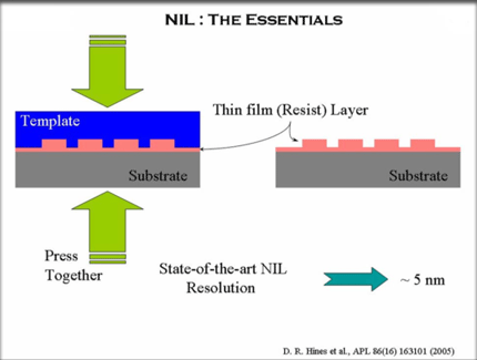
Nano Imprint / UMD
This type of lithography is incredibly simple. This method is simply using a thermoplastic polymer coated onto the substrate (such as a silicon wafer), and then a mold is pressed down on the wafer to print a pattern. Once this is done, a pattern transfer technique such as plasma etching is used to etch away the resist as necessary to expose the pattern on the wafer.
While this technique is simple and can easily be used as a next generation lithography tool, there are also a number of flaws involved with this process. If the imprinting isn't done in a vacuum, there is a high likelihood that the mold will have air bubbles that alter the pattern in unpredictable ways. In addition, the template is susceptible to wear and tear, which means that resolution is lost as the mold is repeatedly used in imprinting. The imprint mold must also take into account uneven depth of imprinting based on the density of the pattern used and potential stretching of the resist. Finally, making the template itself requires extremely precise lithography, which means that it's limited by current generation lithography techniques in resolution. This isn't a solution by itself, which means it can only be used in conjunction with other methods.
Electron Beam Lithography
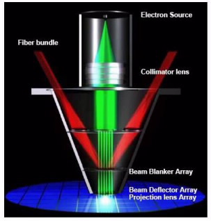
Electron Beam Lithography / SEMI
Just as we saw in the progression of microscopes, the early days were mostly focused on improving light microscopy with higher NA lenses and oil immersion, but today some of the highest resolution microscopes use electrons instead of photons. Similarly, electron beam lithography can generate some of the highest resolutions possible out of all the lithography techniques we've discussed in this article. This means that sub-10nm resolution is easily achieved. In fact, it's fully possible to do away with the resist and simply write the pattern directly on the silicon wafer, eliminating the resist as a potential bottleneck for resolution.
Unfortunately, this system is extremely slow. Rather than the 100+ wafers per hour of current photolithography techniques, electron beam lithography is often limited to less than ten wafers per hour. Using a single electron beam to write an entire 300mm wafer would take around 22 years. While thousands of beams can be simultaneously writing to the wafer to speed up the process, the electrons begin to affect the trajectory of other electrons in other beams. This requires complex modeling to compensate for such effects.
As with EUV lithography, shot noise becomes a significant issue despite a much easier ability to control the dose. This is because even small variations in the number of electrons can significantly effect the roughness of the lines drawn by the electron beam. There is also a strong need to choose a balanced energy for the electron, as excessively energetic electrons can cause significant secondary electron generation, but too little energy means the electrons are easily scattered. Both reduce resolution and can result in unacceptable defects for smaller process nodes.


77 Comments
View All Comments
danjw - Thursday, October 9, 2014 - link
I am wondering if we haven't already hit the limits of current technology. TSMC doesn't seem to be able to produce anything more powerful than a SOC for phones and tablets on their 20nm process. While Intel seems to think they will have 14nm desktop and notebook parts out in the second quarter of next year, I wonder if they really will. Right now all we have seen from them at 14nm is similar to what TSMC is able to do at 20nm.This really concerns me as far as technology stagnating until the next big thing comes along.
Homeles - Thursday, October 9, 2014 - link
There's no end in sight. About a year ago, perhaps a little earlier, the 7 or 5nm nodes were seen as the end of Moore's Law. Advancements have been made since then, though, and scaling past the 5nm node is very likely. 10nm's "recipe" is basically all finished at Intel at this point, with "all" that's left to do at this point being increasing the yields. EUV is making good progress, finally, and should be ready for insertion at Intel's 7nm node (if they skipped it for 10nm, which they likely did).14nm has been in production for quite some time now, with Broadwell first landing in tablets later this month. The chances that Broadwell won't make it to the desktop and notebook market around the middle of next year are essentially zero.
We're still also on schedule to have 450mm wafers introduced by the end of the decade, which would reduce costs by ~30%.
Even not looking at Intel, TSMC has millions of 20nm-based products on the market right now. 20nm is roughly twice as dense as its 28nm predecessor. It doesn't really make sense to be so skeptical of progress, given that the proof pudding has already been delivered.
danjw - Thursday, October 9, 2014 - link
All those 20nm products are not desktop or notebook CPUs or GPUs, which they lead AMD and Nvidia to believe they would be able to do. Intel is way behind its original estimates to get Broadwell out, and that just in table SOCs. Intel wanted badly to get Broadwell parts out for the new school year, then it was Christmas, now it is Q2 of 2015. Yes, I think there is plenty of reason to be skeptical.EMM81 - Monday, October 13, 2014 - link
Your facts are all incorrect...If you can produce an SOC you already have all of the capability to produce GPU's or CPU's since it has logic, SRAM and graphics components already. Broadwell parts are already in the hands of vendors NOW and are being sold this year and they are not SOC's they are low power full core chips. 14nm Broadwell chips are in no way equivalent to 20nm TSMC chips. A fab can use the additional capability of a new node in different ways. They can reduce density to make chips cheaper to make, increase performance, decrease power and all of these things will be done in different ratios depending on the product. You need to work on detailed reasoning and apples to apples comparisons.errorr - Thursday, October 9, 2014 - link
The problem is that the only real advancements are more expensive per transistor and I doubt they will change.The great thing about process shrinks is that it reduces the cost per transistor.
Also I doubt EUV will ever work. It has been almost ready and a couple years away for a decade. Tell me when you don't need MW levels of power to get usable light to a wafer and maybe I will consider it.
450mm wafers have also been just a couple years away for at least 15 years. I'll believe the 2020 hype when I actually see it.
The way to the next node is easy and everyone knows they can use triple patterning. Nobody wants that because of the expense is huge already and every single circuit would have to be redrawn due to limitations on the pokygons.
I don't know what's next but the only people expecting EUV to pan out are the people who have spent billions trying to make it work and failing.
ShieTar - Friday, October 10, 2014 - link
EUV is not "almost ready", it has been commercially available for 2 years now.http://www.zeiss.com/semiconductor-manufacturing-t...
Khenglish - Thursday, October 9, 2014 - link
The problem with smaller processes is not physically producing them. The problem is that they start getting slower than larger processes. This is due to 2 reasons.1. Narrower, more resistive interconnects.
2. Increase in channel doping levels due to not having enough dopant atoms to form a P-N junction as processes increase.
1. As process sizes shrink, so do interconnects. Resistance is dependent on cross sectional area and length of the wire. As you shrink a process, the cross sectional area drops at a squared rate, while length drops at a linear rate. The end result is that wires become linearly more resistive as the process shrinks. Keeping wire length down due to resistance is also a big reason why individual core transistor counts have not been going up significantly. The cores need to stay small to keep the wire length down. Repeaters to boost current drive ability on long wires has been around starting at around 90nm.
2. If you want a 10nm process, you probably have a gate length of 10nm. The volume of a 10nm cube is 10^-18 cm^-3. High doping levels are those above around 10^17 atoms per cm. If we take a high doping level of say 10^18 atoms per cm, then we have only one single dopant atom in the entire channel region of the transistor. This means that if you are one atom off, you lose a transistor, which is difficult not to do with over 1B transistors in a microprocessor. You can dope up to around 10^21 cm^-3, but then your electron and hole mobility are terrible. Mobility is directly proportional to how much current a transistor can push, so as mobility drops performance drops. See this link for what happens to mobility as dopant levels increase.
http://ecee.colorado.edu/~bart/book/mobility.gif
abufrejoval - Saturday, October 11, 2014 - link
From what I read the problem isn't as much phyiscal or technical feasability as economical viability: Moore's law was mostly about the ability to deliver more power at a lower price for the end consumer pushing the technology. Now the economical yields of process shrinks are diminishing to the point where further shrinks won't pay for themselves.DanNeely - Thursday, October 9, 2014 - link
If you're also interested in how simpler transistors are made; hack-a-day's hosted a video lecture from someone who was producing chips with a handful of transistors on them in her home lab a few years ago.http://hackaday.com/2010/03/10/jeri-makes-integrat...
anexanhume - Thursday, October 9, 2014 - link
Graphene isn't dead in the water. There are ways to create a bandgap, for example using bilayer graphene and introducing a gap via electric fields or doping.http://www-als.lbl.gov/index.php/contact/56-bilaye...
Then you can take advantage of its remarkable carrier mobility. Mass production remains a huge issue, and I also have concerns about its effect on living creatures and the environment. http://www.gizmag.com/graphene-bad-for-environment...