Samsung SSD 850 Pro (128GB, 256GB & 1TB) Review: Enter the 3D Era
by Kristian Vättö on July 1, 2014 10:00 AM EST3D NAND in Numbers: Is it Economical?
As with all new semiconductor technologies, the one big question is whether it is economical. There are a ton of memory technologies that have better characteristics than 2D NAND (MRAM and ReRAM to name a couple) but none of them is currently scalable enough to challenge NAND in cost. IMFT's 16nm node is the smallest node shipping in volume, so let's compare Samsung's second generation V-NAND to that to see how it stacks up.
I am basing my analysis on Andrew Walker's blog post from 3DInCites. He is a respected analyst in 3D technologies and his blog post is based on Samsung's and Micron's presentations at the 2014 International Solid-State Circuits Conference, so the data should be as accurate as it can be.
Update 7/8: I was able to find some more accurate data regarding the die size, so I've updated this section with the new data.
| Samsung 2nd Gen V-NAND | Micron 16nm NAND | |
| Process Node | 40nm | 16nm |
| # of Layers | 32 | - |
| Die Capacity | 86Gbit | 128Gbit |
| Die Size | 95.4mm2 | 173mm2 |
| Cell Size | 40,300nm2 | 1,312nm2 |
The only downside of Walker's data is that it only covers Samsung's first generation V-NAND, which was a 24-layer design with a die size of 133mm2 and capacity of 128Gbit. Fortunately, the second generation V-NAND is using the same 40nm node, so the only substantial difference between the first and second generation is the number of layers. The 86Gbit die capacity is certainly a bit odd but it actually makes sense as it is simply the first generation die cut in half with the added layers [(128Gbit / 2) * (32 / 24)]. As such, it is relatively safe to assume that the other variables (cell size etc.) are the same as with the first generation and that is what the table above is based on.
Update 7/8: Actually, the peripheral circuitry does not scale with the memory array, meaning that the die size is actually quite a bit larger than I originally thought.
Before we go deeper with the density analysis, I want to explain how cell size is calculated. As you can see, the figures are way too big to make any sense if you just look at the 40nm and 16nm figures because no matter how you try to multiply them, the results do not make sense.
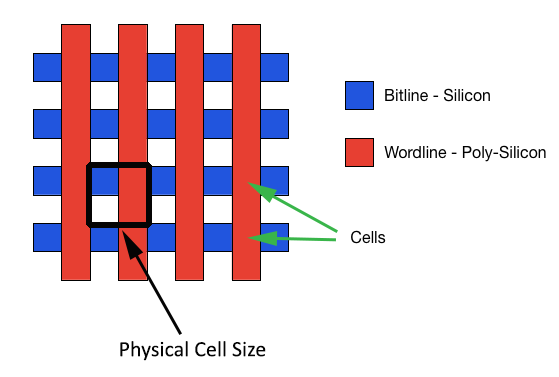
Oftentimes when cell size is discussed, it is only the actual size of the cell that is taken into account, which leaves the distance between cells out of the conclusion. However, the so called empty parts (they are not really empty as you saw in the X-ray a couple of pages back) take a part of the die area similar to the cells, meaning that they cannot be excluded. The appropriate way to measure cell size is from the inner corner of a cell to the outer corners of neighbouring cells in both X and Y axes. This is demonstrated by the black square on the above graph.

With the proper measurements, this is how V-NAND compares to 16nm NAND when just looking at cell size alone (i.e. excluding how the layers impact density). Doesn't look too good, huh?
If you are wondering where the 16nm comes from, it is mostly just marketing. 16nm refers to the smallest length (or resolution as it is often called) in the die, meaning that it is the finest line that can be printed. In the case of NAND, that can either be the wordline or bitline, or the distance between them. With Micron's 16nm NAND, that is likely the length of the wordline and the distance between two wordlines as the two are 32nm when combined (i.e. 16nm each).

The actual cell size did not make justice to V-NAND because the whole idea behind the move to 3D NAND is to increase the cell size and distances between cells to get rid of the issues 2D NAND has. In the graph above, I took the amount of layers into account because you essentially need 32 2D NAND cells to achieve the same density as with 32-layer V-NAND and the game totally changes.
The math behind that graph is just a couple of simple arithmetic equations. The actual cell area is 40,300 (155nm*260nm), meaning that the relative cell area is simply the actual cell area divided by the number of layers. That gives us 1,259nm2(40,300nm2 / 32). To get the relative dimensions, the actual dimensions are divided by the square root of the number of layers (e.g. 155nm / √32 = 27nm).
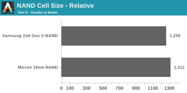
In the end, the relative cell size turns out to be smaller than Micron's 16nm NAND. The difference is not huge (~4%) but when the performance, power consumption and endurance advantages are taken into account, V-NAND is a clear winner.
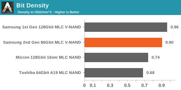
Another way to look at cost efficiency is the bit density. While cell size is a good measure, it does not take peripheral circuitry and ECC/spare bytes into account, which take a part of the die as well. Bit density is simply die capacity divided by die size and it gives us a number for quick and easy comparison.
In this comparison, V-NAND is the leader without any doubts. The bit density is as much as 73% higher, resulting in a much more cost efficient design. The reason why the difference between cell size and bit density is so large is that 2D NAND requires a lot more die area for ECC bytes because it is more error prone. With V-NAND there is less ECC needed thanks to its higher reliability. In addition, Micron's peripheral circuitry design is relatively die consuming, so I wonder how Toshiba's/SanDisk's 15nm stacks up with V-NAND as they are claiming to have a more efficient peripheral circuitry design.
Update 7/8: V-NAND is still denser than the latest 2D NAND nodes but the difference is not overwhelming.
All in all, there is a lot more than just cell area and bit density when it comes to cost efficiency. Yield and equipment cost are two major factors, which are both better for 2D NAND as it is a well known technology and some of the machinery can be reused when moving from one node to another.


160 Comments
View All Comments
GTVic - Tuesday, July 1, 2014 - link
Wondering if the 3D V-NAND has an effect on heat produced by each chip?Laststop311 - Wednesday, July 2, 2014 - link
If only this drive would of been a pci-e 3.0 x4 interface with nvme. We would of finally had a worthy upgrade. Yes it's performance is better than the 840 evo but you can get the 840 evo 1tb for 400 dollars even less if you catch it on sale. So you can get 2x 1tb 840 evo for almost the same price as 1 850 pro. If you compare an 840 evo with 25% OP to a regular 7% on the 850 the 840 evo looks just as good so 2x 825GB drives with 25% OP on each drive costs you 750-800 depending on the deal you get vs 700 for 1000GB. I would rather pay 800 for 1650GB than 700 for 1000GB with performance being nearly identical. I get an extra 650GB (which at 50 cents per GB is another 325 dollars worth of ssd) and tons of over provisioning to give the drive equal or better performance for only 100 dollars more (possibly less as the 840 evo has often sales)Sorry Samsung but 2x 1tb 840 evos with 25% provisioning gives me better or equal performance and a whole 650GB of extra storage for only 100 dollars more. At 50 cents per GB you get 325 dollars worth of more storage capacity for only 100 dollars more and thats with the 25% over provisioning which basically negates the performance increase of the new drives.
The only way samsung could of made this drive worth that money is if they had the drive on a pci-e 3.0 x4 interface with nvme instructions. I'm sure there will be tons of idiots who just buy it cause it's the latest drive. But if you use your brain you can see the 840 evo is still the best SATA drive when the cost/performance ratio is taken into account. 2x 1tb evo's in 25% OP mode gives you 1650GB and costs u 100 dollars extra or less and gives you the same performance or even better compared to 7% 850 pro 1000GB especially when raid 0 is taken into account. I'll take 1650GB over 1000GB if it's only 100 more and performance is equal or better easy choice.
Laststop311 - Wednesday, July 2, 2014 - link
Since samsung is stacking vertically now what they should of done is made a super huge 2tb drive to differentiate themselves from all these other drives. A 2tb drive for 1400 is a little more acceptable than 1tb for 700 simply because it's the only single drive with 2TB capacity.I can see great things happening with vertical stacked nand tho. When this process matures we should be seeing nand drives surpass spinning hard drives in capacity. When samsung has those 1tbit dies its planning for 2017 we should be able to have 8-12TB SSD's
althaz - Wednesday, July 2, 2014 - link
It's a new product and it's priced highly. Eager early adopters who want to move on to the latest and greatest will buy now, value-concious people will buy the 840s. Inventory of the 840s will get eaten up and the 850s will drop in price.This is what happens whenever any product is released, basically ever.
asmian - Wednesday, July 2, 2014 - link
Sorry, but neither this nor the EVO will get my money. Performance is all very well, even if only a tiny handful of users with extremely niche workloads will ever notice any difference, but all this extra reliability at a price premium means NOTHING without simple power loss protection. Restricting something so basic to "Enterprise" class products is the real gouging here by Samsung, not the price.If Crucial can provide that protection on the CHEAPEST drives in their class (M500/M550 and IIRC MX100 too) with performance that is not gimped as a balance, then there is no excuse for Samsung not to. This should be a no-compromise baseline for all SSDs going forward, and Anandtech should push hard for that - users should as well, by voting with their wallets and refusing to buy drives, however fast and powerful, that do not provide power loss protection as a basic feature.
bsd228 - Wednesday, July 2, 2014 - link
Though I agree it is a highly useful feature, it is far less significant to those of us using a good UPS. So I can't agree that it's a no compromise feature.romrunning - Wednesday, July 2, 2014 - link
What you aren't taking into account is the fact that the 850 Pro has MUCH higher endurance, and it's also more consistent. Those two items bring it more into the Intel DC 3500/3700 series type of class. It's not just a sheer performance comparison....and if you thing the 850 Pro is expensive, price out the larger Intel DC S3700 drives.
FunBunny2 - Wednesday, July 2, 2014 - link
"Real" Enterprise SSDs don't even have an MSRP. You negotiate with the vendor, and hope for the best. Now that Texas Memory is in IBM, and Fusion-io in SanDisk, with Violin likely to go somewhere. The conundrum is V.NAND's impact on flattening the curve between Enterprise and Commodity/Retail. At one time, a mainframe had bespoke 14" behemoth hard drive subsystems (in the case of IBM, run by the equivalent of a PDP-x). In due time, binned commodity 3.5" drives are now used.Samsung could well be the driving force to regularize solid state storage. The remaining issue is whether the file system hand waving will be dumped in favor of direct NVM persistence? Samsung, or whoever, likely couldn't care less.
romrunning - Wednesday, July 2, 2014 - link
It's been enjoyable to see a lot of "new" flash memory storage vendors pop-up. More competition is always good in that enterprise space.I've been looking forward to having more SSDs options available to servers at much better pricing. Solid storage advances have a trickle-down effect. If I can put an array of these Samsung 850 Pros into a server and achieve near "enterprise" performance, then that forces Dell/HP/etc. to drop their own SSD pricing.
watersb - Wednesday, July 2, 2014 - link
Fantastic detail of 3D NAND design and why it matters. Thanks very much!