Samsung SSD 850 Pro (128GB, 256GB & 1TB) Review: Enter the 3D Era
by Kristian Vättö on July 1, 2014 10:00 AM ESTAnandTech Storage Bench 2013
Our Storage Bench 2013 focuses on worst-case multitasking and IO consistency. Similar to our earlier Storage Benches, the test is still application trace based - we record all IO requests made to a test system and play them back on the drive we are testing and run statistical analysis on the drive's responses. There are 49.8 million IO operations in total with 1583.0GB of reads and 875.6GB of writes. I'm not including the full description of the test for better readability, so make sure to read our Storage Bench 2013 introduction for the full details.
| AnandTech Storage Bench 2013 - The Destroyer | ||
| Workload | Description | Applications Used |
| Photo Sync/Editing | Import images, edit, export | Adobe Photoshop CS6, Adobe Lightroom 4, Dropbox |
| Gaming | Download/install games, play games | Steam, Deus Ex, Skyrim, Starcraft 2, BioShock Infinite |
| Virtualization | Run/manage VM, use general apps inside VM | VirtualBox |
| General Productivity | Browse the web, manage local email, copy files, encrypt/decrypt files, backup system, download content, virus/malware scan | Chrome, IE10, Outlook, Windows 8, AxCrypt, uTorrent, AdAware |
| Video Playback | Copy and watch movies | Windows 8 |
| Application Development | Compile projects, check out code, download code samples | Visual Studio 2012 |
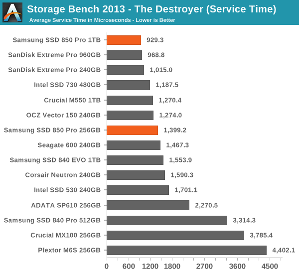
We are reporting two primary metrics with the Destroyer: average data rate in MB/s and average service time in microseconds. The former gives you an idea of the throughput of the drive during the time that it was running the test workload. This can be a very good indication of overall performance. What average data rate doesn't do a good job of is taking into account response time of very bursty (read: high queue depth) IO. By reporting average service time we heavily weigh latency for queued IOs. You'll note that this is a metric we have been reporting in our enterprise benchmarks for a while now. With the client tests maturing, the time was right for a little convergence.
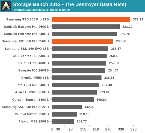
Thanks to the excellent IO consistency, the 850 Pro dominates our 2013 Storage Bench. At the 1TB capacity point, the 850 Pro is over 15% faster than any drive when looking at the average data rate. That is huge because the 850 Pro has less over-provisioning than most of today's high-end drives and the 2013 Storage Bench tends to reward drives that have more over-provisioning because it essentially pushes drives to steady-state. The 256GB model does not do as well as the 1TB one but it is still one of the fastest drives in its class. I wonder if the lesser amount of over-provisioning is the reason or perhaps the Extreme Pro is just so well optimized for mixed workloads.


160 Comments
View All Comments
emvonline - Tuesday, July 1, 2014 - link
is the die size for the NAND chip 67mm^2? I assumed you measured it (pretty easy to do). I would think it would be much larger than thatGigaplex - Tuesday, July 1, 2014 - link
It's difficult to measure the die when multiple of them are on the same package.emvonline - Tuesday, July 1, 2014 - link
send me the package... I promise to have exact die size in a week ..... TEM cross sections in two weeks :-)Kristian Vättö - Tuesday, July 1, 2014 - link
Send me an email at kristian@anandtech.com and let's work this out :)extide - Tuesday, July 1, 2014 - link
Yes, 67mm^2, but remember that is 32 "deep"emvonline - Tuesday, July 1, 2014 - link
@extide: so you measured the die to be 67mm^2? how was this measured ? CSAM? XRAY? that seems odd to use such a small dies for SSD. and that would make it even smaller cell size than the one at ISSCC since it was 134 for a 128Gbit with 24 layers (periphery doesnt shrink as fast with lower density)Kristian Vättö - Tuesday, July 1, 2014 - link
No I didn't because I don't have the equipment to do that. The method I used to calculate the die size is explained on the fifth page of the review:http://www.anandtech.com/show/8216/samsung-ssd-850...
I'm not claiming that it is an accurate figure, hence the "~" sign in front of it. However, Samsung wouldn't disclose the die size when I asked them during the Q&A, so at this point I don't know for sure. However, I have a picture of the 32-layer wafer and once I get back home I'll do the math of the wafer to figure out the exact die size.
emvonline - Tuesday, July 1, 2014 - link
Got it thanks. I am mainly wondering about redundancy, extra blocks and ECC overhead.drwho9437 - Tuesday, July 1, 2014 - link
The micrograph you say is an "x-ray", is almost certainly a transmission electron microscopy image. Given the oxides are light it is a bright field image. It could technically be a SEM image but the resolution is a bit to high, so it most likely is a STEM image with a bright field detector.GTVic - Tuesday, July 1, 2014 - link
Perhaps time should be added as a cost efficiency factor. Presumably the die has to stay in the process much longer due to all the layers being added one at a time.