AMD Radeon HD 7970 Review: 28nm And Graphics Core Next, Together As One
by Ryan Smith on December 22, 2011 12:00 AM EST- Posted in
- GPUs
- AMD
- Radeon
- ATI
- Radeon HD 7000
Meet the Radeon HD 7970
Now that we’ve had a chance to discuss the features and the architecture of GCN and Tahiti, we can finally get to the end result: the card. AMD’s first product in the Southern Islands family is the Radeon HD 7970, continuing AMD’s tradition of launching their fastest single-GPU first.
As we’ve already covered in our discussion on GCN/Tahiti’s architecture, Tahiti shares a lot of physical similarities with Cayman, and so then does the 7970 with the 6970. With the 7970 AMD has targeted a very similar power profile as the 6970, and while AMD has not published the typical board power of the 7970 we know the PowerTune limit is 250W, the same as with the 6970. As a result the 7970 is at least superficially designed to work in the same environments/constraints as the 6970.
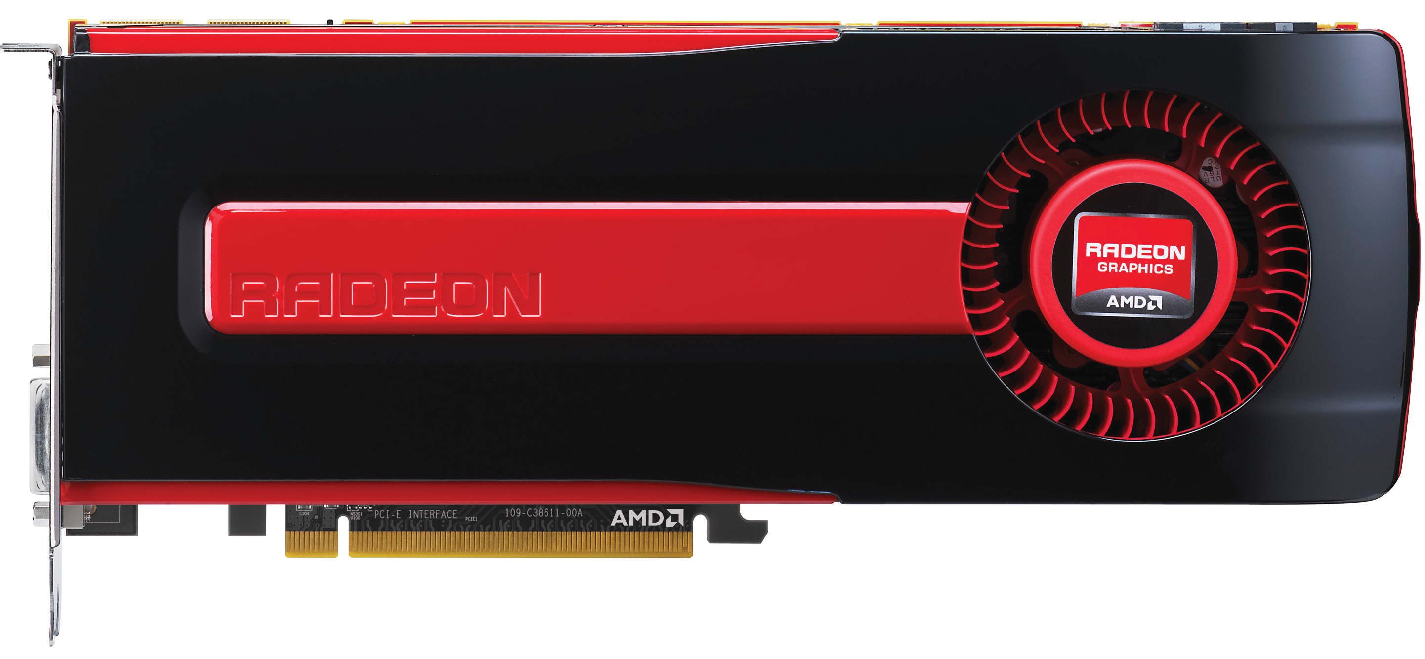
With that said, AMD has not sat idle when it comes to the design of the card – this isn’t just a Tahiti GPU put in a 6970 shell. Livery changes aside it’s clear that the 7970 is a distinct card just from looking at it. AMD’s ill-fated boxy design for their cards is gone; the removable plastic shroud is now once again a rounded design similar to the 5800 series, and this time AMD takes it a step further by slightly rounding off the rear of the card for airflow purposes. Furthermore the shroud is now made of a very hard, very shiny plastic, versus the soft plastic used in past cards.
But the bigger change is on the back of the card, where AMD has completely done away with the backplate. First used in the 5800, backplates help to protect the card from users (and users from the sharp bits of the card), but the tradeoff was that the backplate occupied 2.7mm of space. What’s the significance of 2.7mm? When you’re trying to put these cards adjactent to each other for CrossFire, it’s everything as we have found out.
The boxy design coupled with the backplate meant that the 6900 series used virtually every last millimeter of space they were allowed under the PCIe specification; the cards were so wide that when adjacent it was easy for a card to shift and block the airflow of the neighboring card. The backplate contributed to this problem by consuming 2.7mm of space that could otherwise be used to channel airflow, and as a result it’s gone. AMD’s design doesn’t have the overt wedge that NVIDIA’s does to allow airflow, but it should be enough to keep the cards well enough separated to allow them to breathe when they’re closely together for CrossFire.
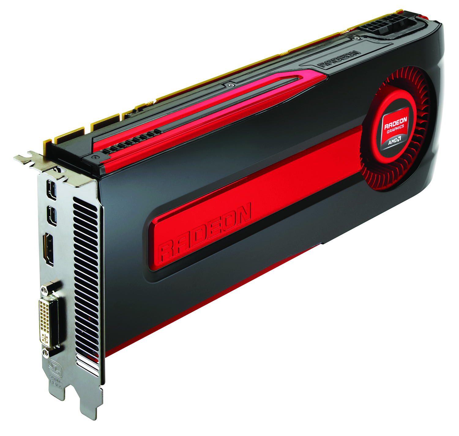
Overall the card is 10.5” going by the PCB, but AMD has a metal reinforcement ring/plate running along the entire card that sticks out the rear. After accounting for this plate the total length of the card is just shy of 11”, making the card roughly half an inch longer than the 6970 and 5870. The difference is not huge, but it will make the 7970 ever so slightly harder to fit than the 6970 in space-constrained cases.
Moving on, while AMD has made some changes to the shrouding to improve cooling, they haven’t stopped there. The blower has also been tweaked slightly compared to what we’ve seen on the 6970. The 7970’s blower is a bit larger (~75mm) and the fins are slightly larger to make use of that space. Overall this should improve the amount of air moved at speeds similar to the blower on the 6970, though AMD didn’t provide any numbers.
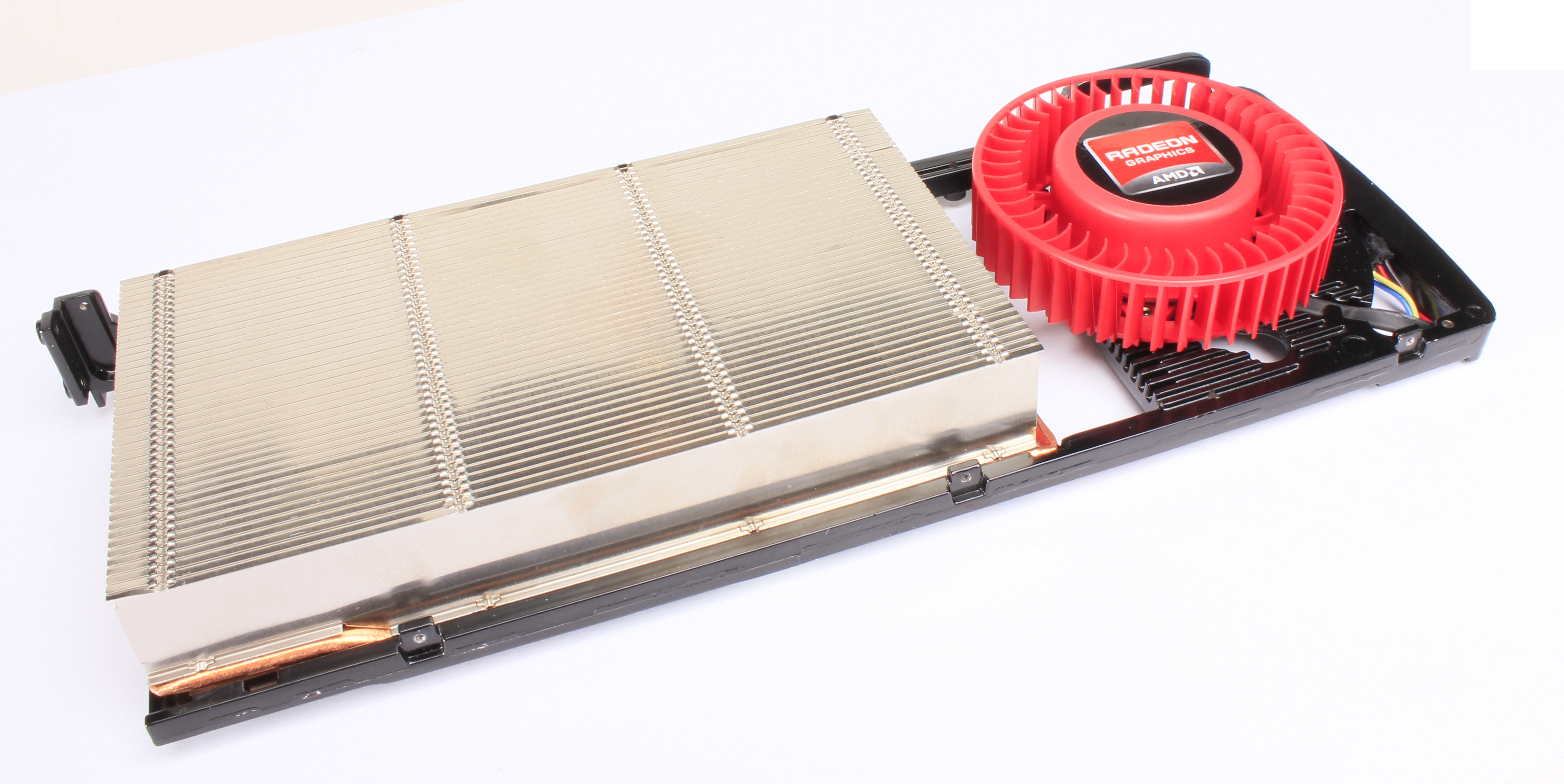
Meanwhile the heatsink is very similar to the 6970’s. As with the 6970 an aluminum heatsink sits on top of a vapor chamber cooler that draws heat from the GPU and other components towards the heatsink. Other than being a bit larger than the 6970 the biggest difference is that AMD is now using the same higher performance phase-change TIM that they used on the 6990, which also means that AMD is highly recommending that the 7970 not be disassembled as the TIM won’t operate nearly as well once it’s been separated. Furthermore as we found out the specific TIM AMD is using is screen printed onto the GPU, so reapplying a new TIM in the same manner is virtually impossible.
Finally, it’s once we move towards the front that we see the biggest change in the name of cooling: AMD has once again moved back to a full slot exhaust vent. As you may recall, starting with the 5800 series AMD moved to a half slot vent configuration so that they could use the other half of the second slot to fit a second DVI port along with their DisplayPort and HDMI ports. The half slot vent did not prove to be a huge problem for the 5800 or 6900 series but it still placed some limits on AMD’s ability to cool their cards and made the process a bit noisier. As the second DVI port has become redundant (more on that later), AMD has opted to get rid of it and go back to using the whole slot for cooling. One way or another though this was probably necessary – looking at our data the 7970 is a bit more power hungry than the 6970 even if the specifications are similar, and as a result AMD needs better cooling to keep parity with the 6970.
Moving on, tweakers will be happy to see that the dual BIOS feature first introduced on the 6900 series is back. The 7970 will feature the same dual BIOS configuration, with a locked factory BIOS (2), and a rewritable BIOS (1) for other uses. As with the 6900 series this is primarily to allow failsafe BIOS flashing, but the implications for GPU unlocking lower tier cards are clear. In fact we’re surprised that AMD included the switch given how rampant 6950 unlocking was, as while it was good PR it must have been bad for their 6970 sales.
Next to the BIOS switch we will find the PCIe power sockets, which given the 250W PowerTune limit of the card mean we’re looking at the same 6+8pin configuration as the 6970. Enthusiasts who caught on to the fact that AMD had to shave some PCIe sockets on the 6900 series should note that the sockets are untouched on the 7970, as the blower now sits above the PCIe sockets. Elsewhere at the front end of the card we’ll find the two CrossFire connectors, and as always when it comes to their high-end cards AMD is supporting up to 3-way CF with the 7970.
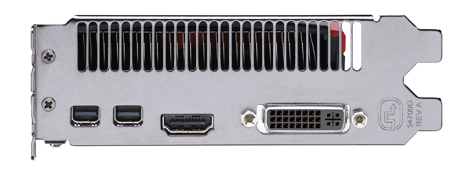
Back to the front of the card we can see AMD’s new Southern Islands port configuration. As you may recall from the 6000 series, with the 6000 series AMD moved from being able to drive 2 dual-link DVI ports (2 sets of paired TMDS transmitters) to being able to drive 1 dual-link DVI port + 1 single-link DVI port, as they removed the 4th TMDS transmitter. Furthermore as AMD has only been able to drive 2 TMDS-type ports at once, the 2nd DVI port was largely redundant as everything it could do the HDMI port could do with a mechanical adaptor.
So for Southern Islands AMD has taken this to its logical conclusion and cut out the 2nd DVI port entirely. There is now a single DL-DVI port, along with an HDMI port and 2 miniDP ports all along a single slot. The 7970 still has the internal logic to drive the same monitor configurations as the 6970, but anyone using the SL-DVI port will now be fed by the HDMI port. In order to make this transition easier on buyers, AMD will be requiring that partners ship both an HDMI to SL-DVI adaptor and an active miniDP to SL-DVI adaptor with their 7970s, so 7970 users will be able to drive up to 3 DVI monitors out of the box, which is actually better than what the 6970 could do. Of course we expect that this will be a limited time offer; once AMD’s partners start putting together cheaper cards later in the 7970’s life, the mDP to SL-DVI adaptor will be the first thing to go.
On that note, for anyone who is curious about idle clockspeeds and power consumption with multiple monitors, it has not changed relative to the 6970. When using a TMDS-type monitor along with any other monitor, AMD has to raise their idle clockspeeds from 350MHz core and 600Mhz memory to 350MHz core and the full 5.5GHz speed for memory, with the power penalty for that being around 30W. Matched timing monitors used exclusively over DisplayPort will continue to be the only way to be able to use multiple monitors without incurring an idle penalty.


Next on the docket we wanted to quickly touch on the subject of RAM. As with their past cards AMD has outfitted the 7970 with RAM rated beyond their memory speed requirements, in this case the 7970 is outfitted with 6GHz modules even though it only needs to operate at 5.5GHz. We haven’t been able to take the card apart so we haven’t seen whose modules AMD is using, but we strongly suspect they’re the same 2Gb Hynix modules the reference 6970 used.
With the move to a 384bit bus AMD has increased the chip count from 8 to 12, and the total RAM size from 2GB to 3GB. As games are only now starting to effectively use more than 1GB of RAM this should offer plenty of headroom for future games, above and beyond even their existing 2GB cards.
At the same time with the move to a 384bit bus this has raised the question of where AMD goes from here. It’s well published that GDDR5 is an intricate memory technology to work with, with the memory bus being the hardest part. To run a 384bit bus at 5.5GHz is quite the accomplishment (NVIDIA didn’t get nearly that high with Fermi), but it also means that we’re near the end of the road for GDDR5. While GDDR5 is rated for up to 7GHz in the real world buses will never be able to scale quite that well and the required memory voltages are on the high side. Meanwhile a 512bit GDDR5 bus is possible but would be even more expensive and difficult than a 384bit bus, and it’s safe to say that’s not the preferred route.
So what comes after GDDR5? At this point AMD tells us that they’re looking at a few different things, but of course it’s far too early to discuss anything in detail. The JEDEC has not passed anything such as a GDDR6 standard, though we expect whatever technology AMD will eventually use will come out of the JEDEC. But if nothing else at this point it’s safe to assume that by the time we’re on 20nm GPUs we won’t be using GDDR5.
Finally, while we haven’t had a chance to tinker with overclocking due to our limited time with the 7970, but AMD is telling us that the 7970 is going to be good overclocker. Most cards should be able to hit 1GHz or higher on the core clock and 6GHz or higher on the memory clock with little effort even with the reference cooler, but the tradeoff will of course be in power consumption and noise, as you’ll need to increase the PowerTune limits to make those overclocks matter.


292 Comments
View All Comments
CeriseCogburn - Thursday, March 8, 2012 - link
Interesting, amd finally copied nvidia..." This problem forms the basis of this benchmark, and the NQueen test proves once more that AMD's Radeon HD 7970 tremendously benefits from leaving behind the VLIW architecture in complex workloads. Both the HD 7970 and the GTX 580 are nearly twice as fast as the older Radeons. "
When we show diversity we should also show that amd radeon has been massively crippled for a long time except when "simpleton" was the key to speed. "Superior architecture" actually means "simple and stupid" - hence "fast" at repeating simpleton nothings, but unable to handle "complex tasks".
LOL - the dumb gpu by amd has finally "evolved".
chizow - Thursday, December 22, 2011 - link
....unfortunately its going to be pitted against Kepler for the long haul.There's a lot to like about Southern Islands but I think its going to end up a very similar situation as Evergreen vs. Fermi, where Evergreen released sooner and took the early lead, but Fermi ultimately won the generation. I expect similar with Tahiti holding the lead for the next 3-6 months until Kepler arrives, but Kepler and its refresh parts winning this 28nm generation once they hit the streets.
Overall the performance and changes AMD made with Tahiti look great compared to Northern Islands, but compared to Fermi parts, its just far less impressive. If you already owned an AMD NI or Evergreen part, there'd be a lot of reason to upgrade, but if you own a Fermi generation Nvidia card there's just far less reason to, especially at the asking price.
I do like how AMD opened up the graphics pipeline with Tahiti though, 384-bit bus, 3GB framebuffer, although I wonder if holding steady with ROPs hurts them compared to Kepler. It would've also been interesting to see how the 3GB GTX 580 compared at 2560 since the 1.5GB model tended to struggle even against 2GB NI parts at that resolution.
ravisurdhar - Thursday, December 22, 2011 - link
My thoughts exactly. Can't wait to see what Kepler can do.Also...4+B transistors? mind=blown. I remember when we were ogling over 1B. Moore's law is crazy.... :D
johnpombrio - Wednesday, December 28, 2011 - link
Exactly. If you look at all the changes that AMD did on the card, I would have expected better results: the power consumption decrease with the Radeon 7970 is mainly due to the die shrink to 28nm. NVidia is planning on a die shrink of their existing Fermi architecture before Kepler is released:http://news.softpedia.com/news/Nvidia-Kepler-Is-On...
Another effect of the die shrink is that clock speed usually increases as there is less heat created at the lower voltage needed with a smaller transistor.
The third change that is not revolutionary is the bump of AMD's 7970's memory bus from 384 bits (matching the 580) from the 6970's 256 bits along with 3GB DDR5 memory vs the GTX580's 1.5GB and the 6970's 2GB.
The final non revolutionary change is bumping the number of stream processors by 33% from 1,536 to 2,048.
Again, breaking out my calculator, the 35% bump in the number of stream processors ALONE causes the increase in the change in the benchmark differences between the 7970 and the 6970.
The higher benchmark, however, does not show ANY OTHER large speed bumps that SHOULD HAVE OCCURED due to the increase in the memory bus size, the higher amount of memory, compute performance, texture fill rate, or finally the NEW ARCHITECTURE.
If I add up all the increases in the technology, I would have expected benchmarks in excess of 50-60% over the previous generation. Perhaps I am naive in how much to expect but, hell, a doubling of transistor count should have produced a lot more than a 35% increase. Add the new architecture, smaller die size, and more memory and I am underwhelmed.
CeriseCogburn - Thursday, March 8, 2012 - link
Well, we can wait for their 50%+ driver increase package+ hotfixes - because after reading that it appears they are missing the boat in drivers by a wide margin.Hopefully a few months after Kepler blows them away, and the amd fans finally allow themselves to complain to the proper authorities and not blame it on Nvida, they will finally come through with a "fix" like they did when the amd (lead site review mastas) fans FINALLY complained about crossfire scaling....
KaarlisK - Thursday, December 22, 2011 - link
What is the power consumption with multiple monitors? Previously, you could not downclock GDDR5, so the resulting consumption was horrible.Ryan Smith - Thursday, December 22, 2011 - link
"On that note, for anyone who is curious about idle clockspeeds and power consumption with multiple monitors, it has not changed relative to the 6970. When using a TMDS-type monitor along with any other monitor, AMD has to raise their idle clockspeeds from 350MHz core and 600Mhz memory to 350MHz core and the full 5.5GHz speed for memory, with the power penalty for that being around 30W. Matched timing monitors used exclusively over DisplayPort will continue to be the only way to be able to use multiple monitors without incurring an idle penalty."KaarlisK - Thursday, December 22, 2011 - link
Thank you for actually replying :)I am so sorry for having missed this.
ltcommanderdata - Thursday, December 22, 2011 - link
Great review.Here's hoping that AMD will implement 64-bit FP support across the whole GCN family and not just the top-end model. Seeing AMD's mobile GPUs don't use the highest-end chip, settling for the 2nd highest and lower, there hasn't been 64-bit FP support in AMD mobile GPUs since the Mobility HD4800 series. I'm interested in this because I can then dabble in some 64-bit GPGPU programming on the go. It also has implications for Apple since their iMacs stick to mobile GPUs, so would otherwise be stuck without 64-bit FP support which presumably could be useful for some of their professional apps.
In regards to hardware accelerated Megatexture, is it directly applicable to id Tech 5's OpenGL 3.2 solution? ie. Will id Tech 5 games see an immediate speed-up with no recoding needed? Or does Partially Resident Texture support require a custom AMD specific OpenGL extension? If it's the later, I can't see it going anywhere unless nVidia agrees to make it a multivendor EXT extension.
Ryan Smith - Thursday, December 22, 2011 - link
Games will need to be specifically coded for PRT; it won't benefit any current games. And you are correct in that it will require and AMD OpenGL extension to use (it won't be accessible from D3D at this time).